 | –≠–ª–µ–∫—Ç—Ä–æ–Ω–Ω—ã–π –∫–æ–º–ø–æ–Ω–µ–Ω—Ç: 20CJQ045 | –°–∫–∞—á–∞—Ç—å:  PDF PDF  ZIP ZIP |

2 Amp
SCHOTTKY RECTIFIER
20CJQ045
PD - 2.478A
The 20CJQ045 surface-mount Schottky rectifier has been
designed for applications requiring very low forward drop and
very small foot prints. Typical applications are in portables,
switching power supplies, converters, automotive systems,
free-wheeling diodes, battery charging and reverse battery
protection.
∑ Small footprint, surface mountable
∑ Low profile
∑ Very low forward voltage drop
∑ High frequency operation
∑ Guard ring for enhanced ruggedness and long-term
reliability
∑ Common Cathode
Description / Features
Characteristics
20CJQ045
Units
I
F(AV)
Rectangular
2.0
A
waveform
V
RRM
45
V
I
FSM
@ tp = 5µs sine
390
A
V
F
@ 1.0Apk, T
J
= 125∞C
0.46
V
(per leg)
T
J
-55 to 150
∞C
Major Ratings and Characteristics
297
SOT-223
CASE STYLE
CASE OUTLINE
NOTES:
1 - DIMENSIONING AND TOLERANCING PER ANSI Y14.5M, 1982.
2 - CONTROLLING DIMENSION: INCH.
3 DIMENSIONS DO NOT INCLUDE MOLD FLASH.
4 - CONFORMS TO JEDEC OUTLINE TO-261AA.
3
2
1
CATHODE
COMMON
COMMON
CATHODE
BASE
ANODE 1
ANODE 2
PART MARKING
CIRCUIT
ATE CODE
INTERNATIONAL
RECTIFIER
LOGO
TOP MARKING
WAFER
LOT CODE
BOTTOM MARKING
PART NUMBER
W
(Y W)
D
Y = LAST DIGIT OF YEAR
WW = WEEK
2CJQF
Next Data Sheet
Index
Previous Datasheet
To Order

298
20CJQ045
Parameters
20CJQ
Units
Conditions
T
J
Max.Junction Temperature Range
-55 to 150
∞C
T
STG
Max. Storage Temperature Range
-55 to 150
∞C
R
thJA
Max. Thermal Resistance, Junction
65
∞C/W
DC operation
to Ambient
R
thJL
Max. Thermal Resistance, Junction
25
∞C/W
DC operation -- see Fig. 4.
to Lead
wt
Approximate Weight
0.13(.0045)
g (oz.)
Case Style
SOT-223
Parameters
20CJQ Units
Conditions
V
FM
Max. Forward Voltage Drop
0.50
V
@ 1.0A
(Per Leg) See Fig. 1
0.62
V
@ 2.0A
0.46
V
@ 1.0A
0.60
V
@ 2.0A
I
RM
Max. Reverse Leakage Current
0.1
mA
T
J
= 25∞C
(Per Leg) See Fig. 2
7.5
mA
T
J
= 125∞C
C
T
Max. Junction Capacitance (Per Leg)
70
pF
V
R
= 5V
DC
, (test signal range 100KHz to 1MHz) 25∞C
L
S
Typical Series Inductance (Per Leg)
6.0
nH
Measured lead to lead 5mm from package body
dv/dt Max. Voltage Rate of Change
7700
V/µs
(Rated V
R
)
Parameters
20CJQ Units Conditions
I
F(AV)
Max. Average Forward Current
2.0
A
50% duty cycle @ T
C
= 126∞C, rectangular waveform
See Fig. 5
4.0
50% duty cycle @ T
C
= 110∞C, rectangular waveform
I
FSM
Max. Peak One Cycle Non - Repetitive
390
A
5µs Sine or 3µs Rect. pulse
Following any rated load condition
Surge Current (Per Leg) See Fig. 7
23
10ms Sine 0r 6ms Rect. pulse
and with rated V
RRM
applied.
E
AS
Non - Repetitive Avalanche Energy
15
mJ
T
J
= 25∞C, I
AS
= 0.2A, L = 750mH
(Per Leg)
I
AR
Repetitive Avalanche Current
0.2
A
Current decaying linearly to zero in 1µsec
(Per Leg)
Frequency limited by T
J
max. V
A
= 1.5 X V
R
typical
Part number
20CJQ045
V
R
Max. DC Reverse Voltage (V)
V
RWM
Max. Working Peak Reverse Voltage (V)
Voltage Ratings
Absolute Maximum Ratings
T
J
= 25∞C
T
J
= 125∞C
V
R
= rated V
R
Thermal-Mechanical Specifications
Electrical Specifications
Pulse Width < 300µs, Duty Cycle < 2%
45
Next Data Sheet
Index
Previous Datasheet
To Order
299
20CJQ045
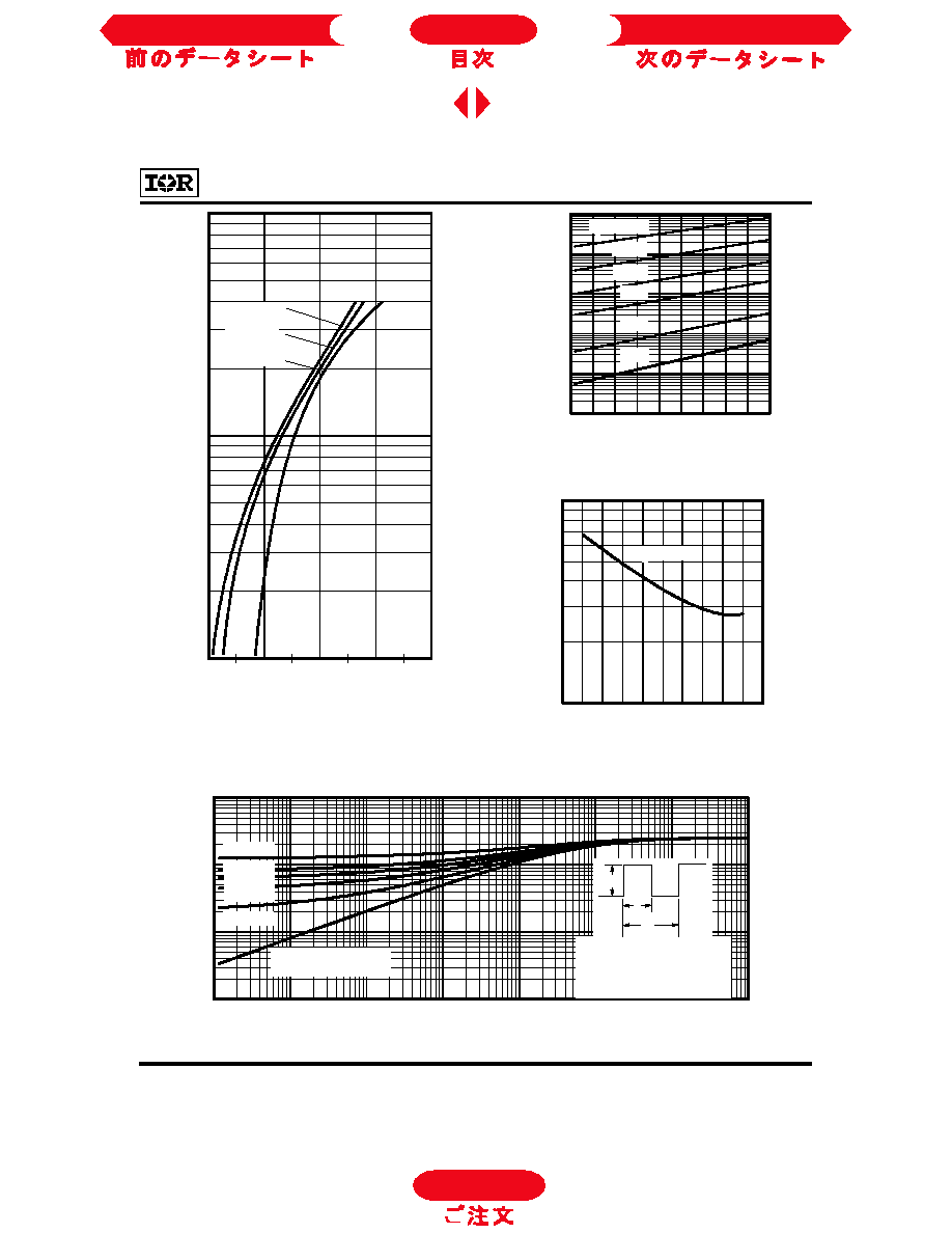
Fig. 1 Max. Forward Voltage Drop Characteristics
(Per Leg)
Fig. 4 Max. Thermal Impedance Z
thJL
Characteristics (Per Leg)
Fig. 3 Typical Junction CapacitanceVs. Reverse
Voltage (Per Leg)
Fig. 2 Typical Values of Reverse Current Vs.
Reverse Voltage (Per Leg)
0.1
1
10
0.2
0.4
0.6
0.8
1.0
FM
F
I
n
s
t
a
n
t
a
n
e
o
u
s
F
o
r
w
a
r
d
C
u
r
r
e
n
t
-
I
(
A
)
Forward Voltage Drop - V (V)
T = 150∞C
T = 125∞C
T = 25∞C
J
J
J
0.0001
0.001
0.01
0.1
1
10
0
5
10
15
20
25
30
35
40
45
R
R
100∞C
75∞C
50∞C
25∞C
Reverse Voltage - V (V)
R
e
v
e
r
s
e
C
u
r
r
e
n
t
-
I
(
m
A
)
125∞C
A
T = 150∞C
J
10
100
0
10
20
30
40
50
T = 25∞C
J
Reverse Voltage - V (V)
R
T
J
u
n
c
t
i
o
n
C
a
p
a
c
i
t
a
n
c
e
-
C
(
p
F
)
A
0.1
1
10
100
0.00001
0.0001
0.001
0.01
0.1
1
10
100
1
Single Pulse
(Thermal Resistance)
t , Rectangular Pulse Duration (Seconds)
D = 0.50
D = 0.33
D = 0.25
D = 0.17
D = 0.08
A
T
h
e
r
m
a
l
I
m
p
e
d
a
n
c
e
-
Z
(
∞
C
/
W
)
2
t
1
t
P
D M
N o te s:
1 . D uty fac tor D = t / t
2 . P e ak T = P x Z + T
J
D M
2
1
thJ L
t
h
J
L
L
To Order
Next Data Sheet
Index
Previous Datasheet

300
20CJQ045
Fig.7 Max. Non-Repetitive Surge Current (Per Leg)
Refer to the Appendix Section for the following:
Appendix D:
Tape and Reel Information -- See page 340.
Fig. 8 Unclamped Inductive Test Circuit
C U R R E N T
M O N IT O R
H IG H -S P E E D
S W IT C H
L
D U T
R g = 2 5 oh m
V d = 25 V o lt
+
B R D
F R E E -W H E E L
D IO D E
4 0H F L 40 S 0 2
Fig. 6 Forward Power Loss Characteristics
(Per Leg)
Fig. 5 Max. Allowable Case Temperature Vs.
Average Forward Current (Per Leg)
80
100
120
140
160
0.0
1.0
2.0
3.0
4.0
DC
A
l
l
o
w
a
b
l
e
C
a
s
e
T
e
m
p
e
r
a
t
u
r
e
-
(
∞
C
)
F(AV)
A
Average Forward Current - I (A)
20CJQ045
R (DC) = 25∞C/W
thJL
0
1
2
3
0
0.4
0.8
1.2
1.6
A
v
e
r
a
g
e
P
o
w
e
r
L
o
s
s
-
(
W
a
t
t
s
)
F(AV)
D = 0.08
D = 0.17
D = 0.25
D = 0.33
D = 0.50
RMS Limit
DC
A
Average Forward Current - I (A)
10
100
1000
10
100
1000
10000
At Any Rated Load Condition
And With Rated V Applied
Following Surge
RRM
N
o
n
-
R
e
p
e
t
i
t
i
v
e
S
u
r
g
e
C
u
r
r
e
n
t
-
I
(
A
)
F
S
M
Square Wave Pulse Duration - t (microsec)
p
A
A
To Order
Next Data Sheet
Index
Previous Datasheet