 | –≠–ª–µ–∫—Ç—Ä–æ–Ω–Ω—ã–π –∫–æ–º–ø–æ–Ω–µ–Ω—Ç: 20MT120UF | –°–∫–∞—á–∞—Ç—å:  PDF PDF  ZIP ZIP |

20MT120UF
V
CES
= 1200V
I
C
= 40A
T
C
= 25∞C
∑
UltraFast Non Punch Through (NPT)
Technology
∑ Positive V
CE(ON)
Temperature Coefficient
∑ 10µs Short Circuit Capability
∑ HEXFRED
TM
Antiparallel Diodes with
UltraSoft Reverse Recovery
∑ Low Diode V
F
∑ Square RBSOA
∑ Aluminum Nitride DBC
∑ Very Low Stray Inductance Design for
High Speed Operation
∑ UL approved (File E78996)
Features
Absolute Maximum Ratings
"FULL-BRIDGE" IGBT MTP
V
CES
Collector-to-Emitter Breakdown Voltage
1200
V
I
C
Continuos Collector Current
@ T
C
= 25∞C
40
A
@ T
C
= 106∞C
20
I
CM
Pulsed Collector Current
100
I
LM
Clamped Inductive Load Current
100
I
F
Diode Continuous Forward Current
@ T
C
= 106∞C
25
I
FM
Diode Maximum Forward Current
100
V
GE
Gate-to-Emitter Voltage
± 20
V
V
ISOL
RMS Isolation Voltage, Any Terminal to Case, t = 1 min
2500
P
D
Maximum Power Dissipation (only IGBT)
@ T
C
= 25∞C
240
W
@ T
C
= 100∞C
96
Parameters
Max
Units
UltraFast NPT IGBT
∑
Optimized for Welding, UPS and SMPS
Applications
∑ Rugged with UltraFast Performance
∑ Benchmark Efficiency above 20KHz
∑ Outstanding ZVS and Hard Switching
Operation
∑ Low EMI, requires Less Snubbing
∑ Excellent Current Sharing in Parallel
Operation
∑ Direct Mounting to Heatsink
∑ PCB Solderable Terminals
∑ Very Low Junction-to-Case Thermal
Resistance
Benefits
M
MTP
5/
I27124 rev. D 02/03
1
www.irf.com

2
20MT120UF
I27124 rev. D 02/03
www.irf.com
V
(BR)CES
Collector-to-Emitter Breakdown Voltage 1200
V
V
GE
= 0V, I
C
= 250µA
V
(BR)CES
/ Temperature Coeff. of
+1.3
V/∞C
V
GE
= 0V, I
C
= 3mA (25-125∞C)
T
J
Breakdown Voltage
V
CE(ON)
Collector-to-Emitter Saturation Voltage
3.29
3.59
V
V
GE
= 15V, I
C
= 20A
4.42
4.66
V
GE
= 15V, I
C
= 40A
3.87
4.11
V
GE
= 15V, I
C
= 20A T
J
= 125∞C
5.32
5.70
V
GE
= 15V, I
C
= 40A T
J
= 125∞C
3.99
4.27
V
GE
= 15V, I
C
= 20A T
J
= 150∞C
V
GE(th)
Gate Threshold Voltage
4
6
V
V
CE
= V
GE
, I
C
= 250µA
V
GE(th)
/ Temperature Coeff. of
-14
mV/∞C V
CE
= V
GE
, I
C
= 3mA (25-125∞C)
T
J
Threshold Voltage
g
fe
Transconductance
17.5
S
V
CE
= 50V, I
C
= 20A, PW = 80µs
I
CES
Zero Gate Voltage Collector Current
(1)
250
µA
V
GE
= 0V, V
CE
= 1200V, T
J
= 25∞C
0.7
3.0
mA
V
GE
= 0V, V
CE
= 1200V, T
J
= 125∞C
2.9
9.0
V
GE
= 0V, V
CE
= 1200V, T
J
= 150∞C
I
GES
Gate-to-Emitter Leakage Current
±250
nA
V
GE
= ± 20V
Electrical Characteristics @ T
J
= 25∞C (unless otherwise specified)
Parameters
Min Typ Max Units Test Conditions
Q
g
Total Gate Charge (turn-on)
176
264
nC
I
C
= 20A
Q
ge
Gate-Emitter Charge (turn-on)
19
30
V
CC
= 600V
Q
gc
Gate-Collector Charge (turn-on)
89
134
V
GE
= 15V
E
on
Turn-On Switching Loss
513
770
µJ
V
CC
= 600V, I
C
= 20A
E
off
Turn-Off Switching Loss
402
603
V
GE
= 15V, R
g
= 5
, L = 200µH
E
tot
Total Switching Loss
915
1373
T
J
= 25∞C, Energy losses include tail
and diode reverse recovery
E
on
Turn-On Switching Loss
930
1395
µJ
V
CC
= 600V, I
C
= 20A
E
off
Turn-Off Switching Loss
610
915
V
GE
= 15V, R
g
= 5
, L = 200µH
E
tot
Total Switching Loss
1540
2310
T
J
= 125∞C, Energy losses include tail
and diode reverse recovery
C
ies
Input Capacitance
2530
3790
pF
V
GE
= 0V
C
oes
Output Capacitance
344
516
V
CC
= 30V
C
res
Reverse Transfer Capacitance
78
117
f = 1.0 MHz
RBSOA
Reverse Bias Safe Operating Area
full square
T
J
= 150∞C, I
C
= 120A
V
CC
= 1000V, V
p
= 1200V
R
g
= 5
, V
GE
= +15V to 0V
SCSOA
Short Circuit Safe Operating Area
10
µs
T
J
= 150∞C
V
CC
= 900V, V
p
= 1200V
R
g
= 5
, V
GE
= +15V to 0V
Switching Characteristics @ T
J
= 25∞C (unless otherwise specified)
Parameters
Min Typ Max Units Test Conditions
(1)
I
CES
includes also opposite leg overall leakage

3
20MT120UF
I27124 rev. D 02/03
www.irf.com
V
FM
Diode Forward Voltage Drop
2.48
2.94
V
I
C
= 20A
3.28
3.90
I
C
= 40A
2.44
2.84
I
C
= 20A, T
J
= 125∞C
3.45
4.14
I
C
= 40A, T
J
= 125∞C
2.21
2.93
I
C
= 20A, T
J
= 150∞C
E
rec
Reverse Recovery Energy of the Diode
420
630
µJ
V
GE
= 15V, R
g
= 5
, L = 200µH
trr
Diode Reverse Recovery Time
98
150
ns
V
CC
= 600V, I
C
= 20A
Irr
Peak Reverse Recovery Current
33
50
A
T
J
= 125∞C
Thermal- Mechanical Specifications
T
J
Operating Junction Temperature Range
- 40
150
∞C
T
STG
Storage Temperature Range
- 40
125
R
thJC
Junction-to-Case
IGBT
0.35
0.52
∞C/ W
Diode
0.40
0.61
R
thCS
Case-to-Sink
Module
0.06
(Heatsink Compound Thermal Conductivity = 1 W/mK)
Clearance (
external shortest distance in air
5.5
mm
between two terminals)
Creepage (
shortest distance along external
8
surface of the insulating material between 2 terminals
)
T
Mounting Torque
(2)
3 ± 10%
Nm
Wt
Weight
66
g (oz)
Parameters
Min
Typ
Max
Units
Diode Characteristics @ T
J
= 25∞C (unless otherwise specified)
Parameters
Min Typ Max Units Test Conditions
(2) A mounting compound is recommended and the torque should be checked after 3 hours to allow for the spread of the
compound. Lubricated threads

4
20MT120UF
I27124 rev. D 02/03
www.irf.com
Fig. 1 - Maximum DC Collector Current vs.
Case Temperature
Fig. 2 - Power Dissipation vs. Case
Temperature
Fig. 3 - Forward SOA
T
C
= 25∞C; T
J
150∞C
Fig. 4 - Reverse Bias SOA
T
J
= 150∞C; V
GE
=15V
0
20
40
60
80
100 120 140 160
TC (∞C)
0
50
100
150
200
250
P
tot
(W)
0
20
40
60
80
100 120 140 160
TC (∞C)
0
10
20
30
40
50
I C
(A)
10
100
1000
10000
VCE (V)
1
10
100
1000
I C
(A)
1
10
100
1000
10000
VCE (V)
0.01
0.1
1
10
100
1000
I C
(A)
10 µs
100 µs
1ms
DC
5
20MT120UF
I27124 rev. D 02/03
www.irf.com
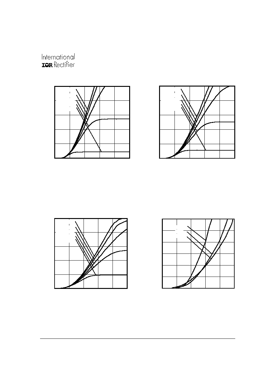
Fig. 6 - Typ. IGBT Output Characteristics
T
J
= 25∞C; tp = 80µs
Fig. 5 - Typ. IGBT Output Characteristics
T
J
= -40∞C; tp = 80µs
Fig. 8 - Typ. Diode Forward Characteristics
tp = 80µs
Fig. 7 - Typ. IGBT Output Characteristics
T
J
= 125∞C; tp = 80µs
0
2
4
6
8
10
VCE (V)
0
20
40
60
80
100
I CE
(A
)
VGE = 18V
VGE = 15V
VGE = 12V
VGE = 10V
VGE = 8.0V
0
2
4
6
8
10
VCE (V)
0
20
40
60
80
100
I CE
(A)
VGE = 18V
VGE = 15V
VGE = 12V
VGE = 10V
VGE = 8.0V
0
2
4
6
8
10
VCE (V)
0
20
40
60
80
100
I CE
(A
)
VGE = 18V
VGE = 15V
VGE = 12V
VGE = 10V
VGE = 8.0V
0.0
1.0
2.0
3.0
4.0
5.0
VF (V)
0
20
40
60
80
100
120
I F
(A
)
-40∞C
25∞C
125∞C