 | –≠–ª–µ–∫—Ç—Ä–æ–Ω–Ω—ã–π –∫–æ–º–ø–æ–Ω–µ–Ω—Ç: 47CTQ020S | –°–∫–∞—á–∞—Ç—å:  PDF PDF  ZIP ZIP |

SCHOTTKY RECTIFIER
40 Amp
PD-20540 rev. E 10/99
1
www.irf.com
Major Ratings and Characteristics
I
F(AV)
Rectangular
40
A
waveform
V
RRM
20
V
I
FSM
@ tp = 5 µs sine
1000
A
V
F
@
20 Apk, T
J
= 125 ∞C
0.34
V
T
J
- 55 to 150
∞C
Characteristics
Values
Units
This center tap Schottky rectifier has been optimized for ultra
low forward voltage drop specifically for 3.3V output power
supplies. The proprietary barrier technology allows for reliable
operation up to 150 ∞C junction temperature. Typical
applications are in parallel switching power supplies,
converters, reverse battery protection, and redundant power
subsystems.
150 ∞C T
J
operation
Center tap configuration
Optimized for 3.3V application
Ultra low forward voltage drop
High frequency operation
Guard ring for enhanced ruggedness and long term
reliability
High purity, high temperature epoxy encapsulation for
enhanced mechanical strength and moisture resistance
Description/Features
Case Styles
47CTQ020
47CTQ020S
47CTQ020-1
TO-220
D
2
PAK
TO-262
4 7 C T Q 0 2 0
47CTQ020S
47CTQ020-1

47CTQ020, 47CTQ020S, 47CTQ020-1
2
PD-20540 rev. E 10/99
www.irf.com
I
F(AV)
Max. Average Forward (Per Device)
40
A
50% duty cycle @ T
C
= 135∞C, rectangular wave form
Current
(Per Leg)
20
I
FSM
Max. Peak One Cycle Non-Repetitive
1000
5µs Sine or 3µs Rect. pulse
Surge Current (Per Leg)
250
10ms Sine or 6ms Rect. pulse
E
AS
Non-Repetitive Avalanche Energy
18
mJ
T
J
= 25 ∞C, I
AS
=3 Amps, L =3 mH
(Per Leg)
I
AR
Repetitive Avalanche Current
3
A
Current decaying linearly to zero in 1 µsec
(Per Leg)
Frequency limited by T
J
max. V
A
= 1.5 x V
R
typical
Following any rated
load condition and with
rated Vrrm
applied
Electrical Specifications
Part number
47CTQ020, ..020S, ..020-1
V
R
Max. DC Reverse Voltage (V) @ 125∞ C
V
R
Max. DC Reverse Voltage (V) @ 150∞ C
Voltage Ratings
Absolute Maximum Ratings
Parameters
47CTQ Units
Conditions
A
T
J
= 25 ∞C
T
J
= 125 ∞C
V
R
= rated V
R
Parameters 47CTQ Units Conditions
T
J
Max. Junction Temperature Range
-55 to 150
∞C
T
stg
Max. Storage Temperature Range
-55 to 150
∞C
R
thJC
Max. Thermal Resistance Junction
1.5
∞C/W DC operation
to Case (Per Leg)
R
thJC
Max. Thermal Resistance Junction
0.75
∞C/W DC operation
to Case (Per Package)
R
thCS
Typical Thermal Resistance, Case
0.50
∞C/W Mounting surface , smooth and greased
to Heatsink (only for TO-220)
wt
Approximate Weight
2 (0.07)
g (oz.)
T
Mounting Torque
Min.
6 (5)
Max.
12 (10)
Thermal-Mechanical Specifications
Kg-cm
(Ibf-in)
(1) Pulse Width < 300µs, Duty Cycle <2%
20
10
T
J
= 150 ∞C
Parameters
47CTQ Units
Conditions
V
FM
Max. Forward Voltage Drop
0.45
V
@ 20A
(Per Leg)
(1)
0.51
V
@ 40A
0.34
V
@ 20A
0.44
V
@ 40A
0.31
V
@ 20A
0.42
V
@ 40A
I
RM
Max. Reverse Leakage Current
3
mA T
J
= 25 ∞C
(Per Leg)
(1)
310
mA T
J
= 125 ∞C
60
mA T
J
= 125 ∞C
V
R
= 5V
45
mA T
J
= 125 ∞C
V
R
= 3.3V
306
mA T
J
= 150 ∞C
V
R
= 10V
V
F(TO)
Threshold Voltage
0.188
V
T
J
= T
J
max.
r
t
Forward Slope Resistance
5.9
m
C
T
Max. Junction Capacitance (Per Leg)
3000
pF
V
R
= 5V
DC
, (test signal range 100Khz to 1Mhz) 25∞C
L
S
Typical Series Inductance (Per Leg)
5.5
nH
Measured lead to lead 5mm from package body
dv/dt Max. Voltage Rate of Change
10,000
V/ µs
(Rated V
R
)
3
PD-20540 rev. E 10/99
www.irf.com
47CTQ020, 47CTQ020S, 47CTQ020-1
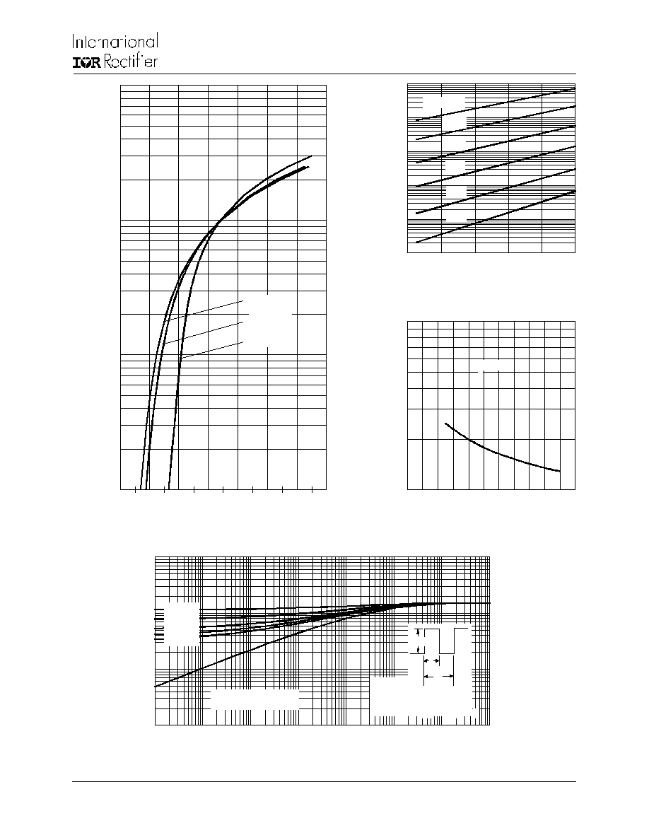
Fig. 2 - Typical Values Of Reverse Current
Vs. Reverse Voltage (Per Leg)
Fig. 3 - Typical Junction Capacitance
Vs. Reverse Voltage (Per Leg)
Fig. 4 - Max. Thermal Impedance Z
thJC
Characteristics (Per Leg)
Fig. 1 - Max. Forward Voltage Drop Characteristics
(Per Leg)
1 000
10 000
0
2
4
6
8
10 12 14 16 18 20 2 2
R
T
J
u
n
c
tio
n
C
a
p
a
c
i
ta
n
c
e
-
C
(
p
F
)
R everse Voltag e - V (V)
T = 25∞C
J
0.01
0.1
1
10
0.00001
0.0001
0.001
0.01
0.1
1
10
100
th
J
C
t , R e ctang ular P ulse D uratio n (Se co nds)
Sing le P u ls e
(The rm al R e sista nc e)
1
T
h
e
r
m
a
l I
m
p
e
d
a
n
c
e
Z
(
∞
C
/
W
)
Notes:
1. D uty factor D = t / t
2. Peak T = P x Z + T
1
2
J
th JC
C
D M
D = 0.75
D = 0.50
D = 0.33
D = 0.25
D = 0.2 0
2
t
1
t
P
D M
0. 01
0.1
1
10
100
10 00
0
4
8
12
16
2 0
R
R
125∞C
100∞C
75∞C
50∞C
25∞C
Re
v
e
r
s
e
C
u
r
r
e
n
t
-
I
(
m
A
)
Re ve rse Vo ltag e - V ( V)
T = 150∞C
J
1
1 0
10 0
100 0
0
0.2
0. 4
0.6
0. 8
1
1.2
1.4
F
F M
T = 150∞C
T = 125∞C
T = 25∞C
J
J
J
Fo rw ard Vo ltag e D ro p - V (V)
I
n
s
t
a
n
t
a
n
e
o
u
s
F
o
rw
a
r
d
C
u
rre
n
t
-
I
(A
)

47CTQ020, 47CTQ020S, 47CTQ020-1
4
PD-20540 rev. E 10/99
www.irf.com
Fig. 7 - Max. Non-Repetitive Surge Current (Per Leg)
Fig. 5 - Max. Allowable Case Temperature
Vs. Average Forward Current (Per Leg)
Fig. 8 - Unclamped Inductive Test Circuit
Fig. 6 - Forward Power Loss Characteristics
(Per Leg)
FR EE -W HEEL
D IO D E
40HFL40S02
C UR R E NT
M ON ITO R
HIG H-SPEED
SW ITC H
IR FP460
L
D UT
R g = 25 ohm
V d = 25 V olt
+
(2) Formula used: T
C
= T
J
- (Pd + Pd
REV
) x R
thJC
;
Pd = Forward Power Loss = I
F(AV)
x V
FM
@ (I
F(AV)
/
D) (see Fig. 6);
Pd
REV
= Inverse Power Loss = V
R1
x I
R
(1 - D); I
R
@ V
R1
= 10 V
1 0 0
1 0 0 0
1 0
1 0 0
1 0 0 0
1 0 0 0 0
FS
M
N
o
n
-
R
e
p
e
t
i
t
i
v
e
S
u
r
g
e
C
u
r
r
e
n
t
-
I
(
A
)
p
A t A ny Rated Lo ad C onditio n
A nd W ith Rated V Applied
Fo llowing Surge
R R M
Square W ave P ulse D uration - t (m icrose c)
0
2
4
6
8
10
12
0
5
10
15
20
25
30
D C
A
v
e
r
a
g
e
P
o
w
e
r
L
o
ss -
(
W
a
t
t
s
)
F(AV )
R M S Lim it
D = 0.20
D = 0.25
D = 0.33
D = 0.50
D = 0.75
A ve rag e Fo rward C urre nt - I (A )
9 0
10 0
11 0
12 0
13 0
14 0
15 0
16 0
0
5
10
15
20
25
30
D C
A
l
l
o
w
a
b
l
e C
a
s
e
T
e
m
p
er
a
t
u
r
e -
(∞
C
)
F(AV )
s e e n o te (2)
A ve rag e Fo rward C urrent - I (A)
Square wave (D = 0.50)
10V applied

5
PD-20540 rev. E 10/99
www.irf.com
47CTQ020, 47CTQ020S, 47CTQ020-1
3.78 (0.15)
3.54 (0.14)
10.54 (0.41)
MAX.
DIA.
15.24 (0.60)
14.84 (0.58)
2.92 (0.11)
2.54 (0.10)
1
TERM 2
14.09 (0.55)
13.47 (0.53)
3.96 (0.16)
3.55 (0.14)
0.94 (0.04)
0.69 (0.03)
4.57 (0.18)
4.32 (0.17)
3
0.61 (0.02) MAX.
5.08 (0.20) REF.
1.32 (0.05)
1.22 (0.05)
6.48 (0.25)
6.23 (0.24)
2∞
0.10 (0.004)
1.40 (0.05)
1.15 (0.04)
2.89 (0.11)
2.64 (0.10)
1
3
2.04 (0.080) MAX.
2
2
Dimensions in millimeters and (inches)
Conform to JEDEC outline TO-220AB
2
BASE
COMMON
CATHODE
1
2
3
ANODE
COMMON
CATHODE
ANODE
1
2
Ordering Information Table
Device Code
1
5
2
4
3
1
-
Essential Part Number
2
-
C = Common Cathode
3
-
T = TO-220
4
-
Q = Schottky Q Series
5
-
Voltage Rating 020 = 20V
6
-
-1 = TO-262
S = D
2
Pak
47
C
T
Q
020 -1
6
Outline Table