 | ÐлекÑÑоннÑй компоненÑ: 50WQ04FN | СкаÑаÑÑ:  PDF PDF  ZIP ZIP |
Äîêóìåíòàöèÿ è îïèñàíèÿ www.docs.chipfind.ru
I
F(AV)
Rectangular
5.5
A
waveform
V
RRM
40
V
I
FSM
@ tp = 5 µs sine
550 A
V
F
@
5 Apk, T
J
= 125°C
0.44
V
T
J
range
- 40 to 150
°C
SCHOTTKY RECTIFIER
5.5 Amp
50WQ04FN
Bulletin PD-20524 rev. F 06/04
1
www.irf.com
Major Ratings and Characteristics
Characteristics
50WQ04FN Units
Description/ Features
The 50WQ04FN surface mount Schottky rectifier has been
designed for applications requiring low forward drop and
small foot prints on PC board. Typical applications are in disk
drives, switching power supplies, converters, free-wheeling
diodes, battery charging, and reverse battery protection.
Popular D-PAK outline
Small foot print, surface moutable
Low forward voltage drop
High frequency operation
Guard ring for enhanced ruggedness and long term
reliability
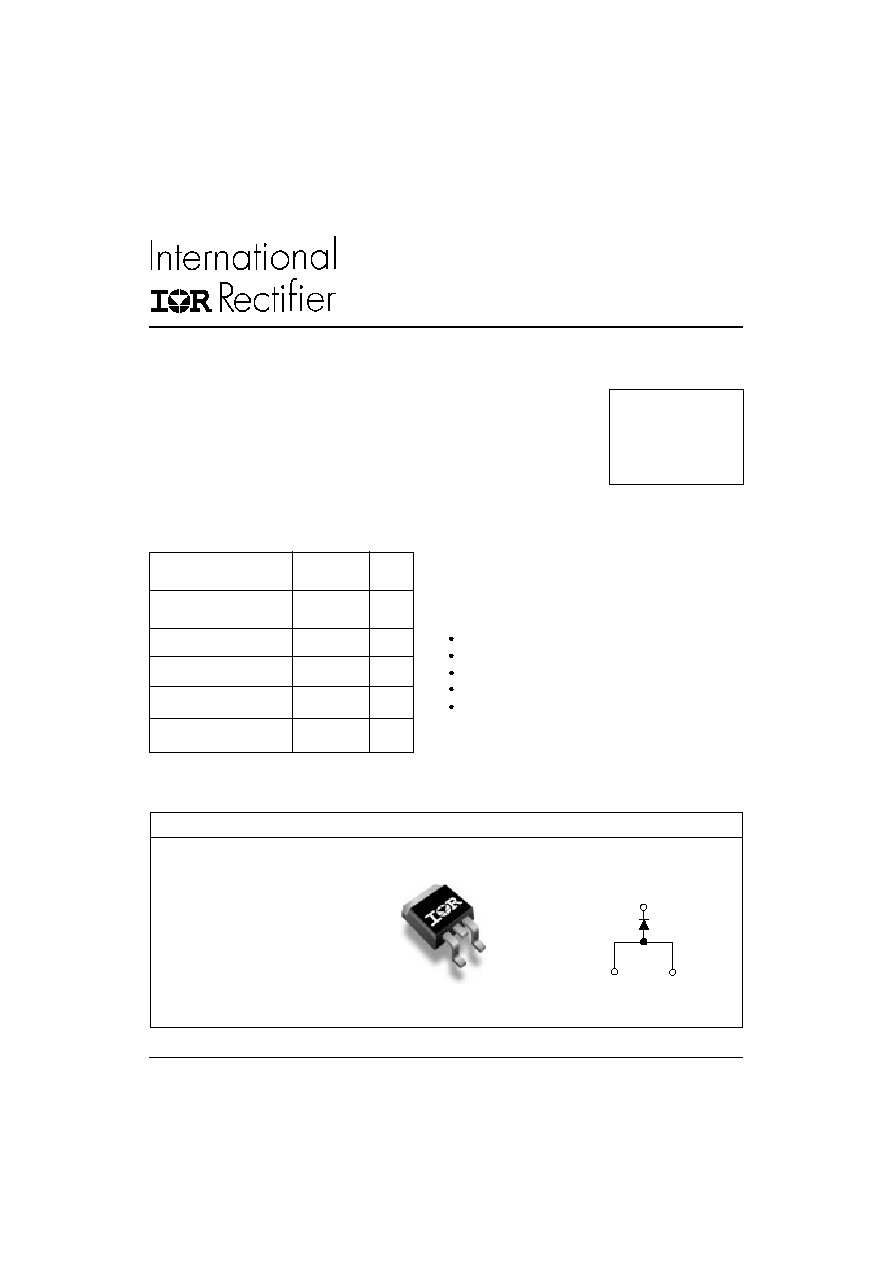
Case Styles
50WQ04FN
D-PAK
I
F(AV)
= 5.5Amp
V
R
= 40V
Anode
1
3
Base
Cathode
Anode
4, 2
50WQ04FN
Bulletin PD-20524 rev. F 06/04
2
www.irf.com
Part number
50WQ04FN
V
R
Max. DC Reverse Voltage (V)
V
RWM
Max. Working Peak Reverse Voltage (V)
40
Voltage Ratings
V
FM
Max. Forward Voltage Drop
0.51
V
@ 5A
* See Fig. 1
(1)
0.63
V
@ 10A
0.44
V
@ 5A
0.59
V
@ 10A
I
RM
Max. Reverse Leakage Current
3
mA
T
J
= 25 °C
* See Fig. 2
(1)
40
mA
T
J
= 125 °C
V
F(TO)
Threshold Voltage
0.27
V
T
J
= T
J
max.
r
t
Forward Slope Resistance
26.77
m
C
T
Typical Junction Capacitance
405
pF
V
R
= 5V
DC
(test signal range 100Khz to 1Mhz) 25 °C
L
S
Typical Series Inductance
5.0
nH
Measured lead to lead 5mm from package body
T
J
= 25 °C
T
J
= 125 °C
V
R
= rated V
R
Electrical Specifications
Parameters
50WQ...
Units
Conditions
(1) Pulse Width < 300µs, Duty Cycle < 2%
I
F(AV)
Max. Average Forward Current
5.5
A
50% duty cycle @ T
C
= 135°C, rectangular wave form
* See Fig. 5
I
FSM
Max. Peak One Cycle Non-Repetitive
550
5µs Sine or 3µs Rect. pulse
Surge Current * See Fig. 7
90
10ms Sine or 6ms Rect. pulse
E
AS
Non-Repetitive Avalanche Energy
9
mJ
T
J
= 25 °C, I
AS
= 1.5 Amps, L = 8 mH
I
AR
Repetitive Avalanche Current
1.2
A
Current decaying linearly to zero in 1 µsec
Frequency limited by T
J
max. V
A
= 1.5 x V
R
typical
Absolute Maximum Ratings
Following any rated
load condition and with
rated V
RRM
applied
A
Parameters
50WQ... Units
Conditions
<
thermal runaway condition for a diode on its own heatsink
(*) dPtot
1
dTj
Rth( j-a)
T
J
Max. Junction Temperature Range (*) -40 to 150
°C
T
stg
Max. Storage Temperature Range
-40 to 150
°C
R
thJC
Max. Thermal Resistance
3.0
°C/W DC operation
* See Fig. 4
Junction to Case
wt
Approximate Weight
0.3 (0.01) g (oz.)
Case Style
D-Pak
Similar to TO-252AA
Device Marking
50WQ04FN
Thermal-Mechanical Specifications
Parameters
50WQ... Units
Conditions
50WQ04FN
Bulletin PD-20524 rev. F 06/04
3
www.irf.com
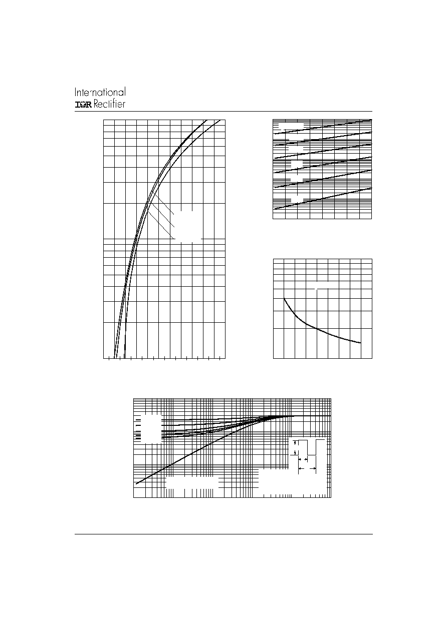
Fig. 2 - Typical Values of Reverse Current
Vs. Reverse Voltage
Fig. 3 - Typical Junction Capacitance
Vs. Reverse Voltage
Fig. 4 - Maximum Thermal Impedance Z
thJC
Characteristics
Fig. 1 - Maximum Forward Voltage Drop Characteristics
0.001
0.01
0.1
1
10
100
0
5
10
15
20
25
30
35
40
R
R
125°C
100°C
75°C
50°C
25°C
R
e
v
e
r
s
e C
u
r
r
en
t
-
I
(
m
A
)
T = 150°C
J
Reverse Voltage - V (V)
100
1000
0
5
10 15 20 25 30 35 40 45
R
T
J
u
nc
t
i
o
n
Ca
p
a
c
i
t
a
nc
e
-
C (
p
F
)
Reverse Voltage - V (V)
T = 25°C
J
0.01
0.1
1
10
0.00001
0.0001
0.001
0.01
0.1
1
th
J
C
t , Rectangular Pulse Duration (Seconds)
Single Pulse
(Thermal Resistance)
1
T
h
e
r
m
a
l
I
m
p
e
d
a
n
c
e
Z
(
°
C
/
W
)
D = 0.75
D = 0.50
D = 0.33
D = 0.25
D = 0.20
J
DM
thJC
C
1
2
2
t
1
t
P
DM
Notes:
1. Duty factor D = t / t
2. Peak T = P x Z + T
1
10
100
0
0.2 0.4 0.6 0.8
1
1.2 1.4 1.6 1.8
2
2.2
I
n
s
t
a
n
tan
e
o
u
s
F
o
r
w
ar
d C
u
r
r
e
n
t
-
I
(
A
)
F
FM
Forward Voltage Drop - V (V)
T = 150°C
T = 125°C
T = 25°C
J
J
J
50WQ04FN
Bulletin PD-20524 rev. F 06/04
4
www.irf.com
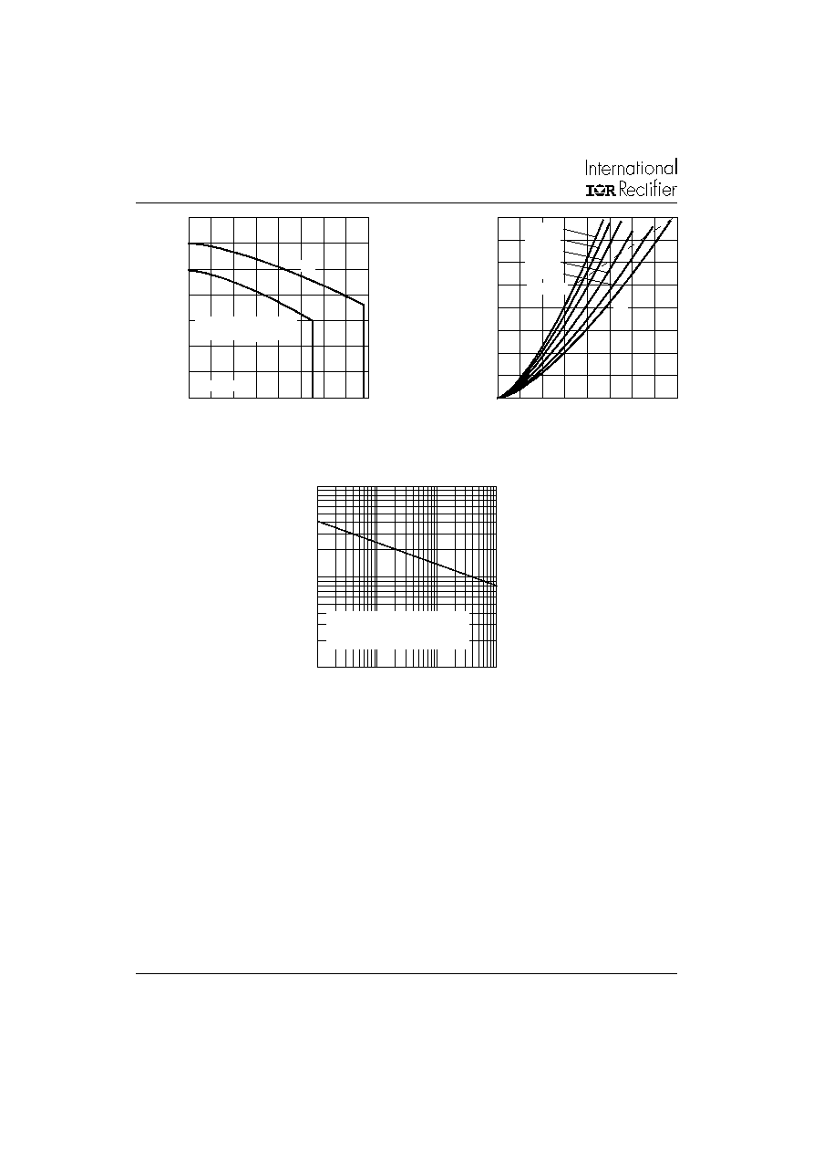
Fig. 5 - Maximum Allowable Case Temperature
Vs. Average Forward Current
Fig. 6 - Forward Power Loss Characteristics
Fig. 7 - Maximum Non-Repetitive Surge Current
(2) Formula used: T
C
= T
J
- (Pd + Pd
REV
) x R
thJC
;
Pd = Forward Power Loss = I
F(AV)
x V
FM
@ (I
F(AV)
/
D) (see Fig. 6);
Pd
REV
= Inverse Power Loss = V
R1
x I
R
(1 - D); I
R
@ V
R1
= 80% rated V
R
120
125
130
135
140
145
150
155
0
1
2
3
4
5
6
7
8
DC
A
l
l
o
w
abl
e
C
a
s
e
T
e
m
p
e
r
at
u
r
e
-
(
°
C
)
F(AV)
see note (2)
Square wave (D = 0.50)
80% Rated V applied
R
Average Forward Current - I (A)
0
0.5
1
1.5
2
2.5
3
3.5
4
0
1
2
3
4
5
6
7
8
DC
A
v
e
r
ag
e
P
o
we
r
L
o
s
s
-
(
W
at
t
s
)
F(AV)
RMS Limit
D = 0.20
D = 0.25
D = 0.33
D = 0.50
D = 0.75
Average Forward Current - I (A)
Square Wave Pulse Duration - t
p
(microsec)
Non-Repetitive Surge Current - I
FSM
(A)
10
100
1000
10
100
1000
10000
At Any Rated Load Condition
And With Rated Vrrm Applied
Following Surge
50WQ04FN
Bulletin PD-20524 rev. F 06/04
5
www.irf.com
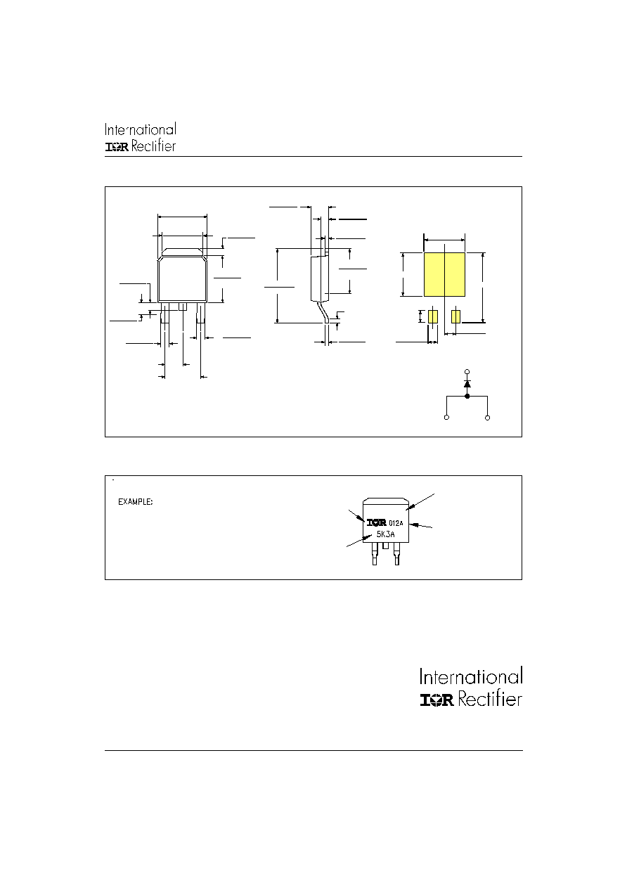
6.73 (0.26)
6.35 (0.25)
5.46 (0.21)
5.21 (0.20)
4
1.27 (0.05)
0.88 (0.03)
5.97 (0.23)
1 - Anode
2 - Cathode
3 - Anode
4 - Cathode
1.64 (0.02)
1.52 (0.06)
1.15 (0.04)
1.14 (0.04)
0.76 (0.03)
2x
2.28 (0.09)
2x
0.89 (0.03)
0.64 (0.02)
3x
4.57 (0.18)
1
2
3
6.22 (0.24)
2.38 (0.09)
2.19 (0.08)
6.45 (0.24)
5.68 (0.22)
10.42 (0.41)
9.40 (0.37)
0.46 (0.02)
0.58 (0.02)
1.14 (0.04)
0.89 (0.03)
0.51 (0.02)
MIN.
0.58 (0.02)
0.46 (0.02)
MINIMUM RECOMMENDED FOOTPRINT
5.97 (0.24)
10.67 (0.42)
1.65 (0.06)
6.48 (0.26)
2x
2.54 (0.10)
2x
2.28 (0.09)
2x
Outline Table
Modified JEDEC outline TO-262AA
Dimensions in millimeters and (inches)
Anode
1
3
Base
Cathode
Anode
4, 2
Marking Information
ASSEMBLED ON WW 12, 2000
IN ASSEMBLY LINE "A"
LOT CODE 5K3A
RECTIFIER
LOGO
LOT CODE
ASSEMBLY
INTERNATIONAL
PART NUMBER
DATE CODE
YEAR 0 = 2000
WEEK 12
LINE A
THIS IS A 50WQ04FN WITH
50WQ04FN
IR WORLD HEADQUARTERS: 233 Kansas St., El Segundo, California 90245, USA Tel: (310) 252-7105
TAC Fax: (310) 252-7309
Visit us at www.irf.com for sales contact information. 06/04
Data and specifications subject to change without notice.
This product has been designed and qualified for Industrial Level.
Qualification Standards can be found on IR's Web site.