 | ÐлекÑÑоннÑй компоненÑ: 52CPQ030 | СкаÑаÑÑ:  PDF PDF  ZIP ZIP |
Äîêóìåíòàöèÿ è îïèñàíèÿ www.docs.chipfind.ru
15.90 (0 .626 )
15.30 (0 .602 )
14.20 (0 .559)
14. 80 ( 0.583)
3. 70 (0.14 5)
4. 30 (0 .17 0)
5.30 ( 0.208)
5. 70 (0.225)
5.50 ( 0.217)
4. 50 (0 .17 7)
(2 PLCS.)
3. 55 (0 .139)
3. 65 (0.144)
2. 20 (0 .08 7)
MAX.
1. 00 (0 .03 9)
1. 40 (0 .05 6)
0. 40 (0.213)
0.80 ( 0.032)
4.70 ( 0.185)
5. 30 (0 .209)
1.5 ( 0.059)
2.5 ( 0.098)
2. 40 (0.095)
MAX.
10 .86 (0.427)
10. 94 ( 0.430)
20 .30 (0.800)
19 .70 (0.775)
DIA.
1
2
3
Characteristics
52CPQ030 Units
Major Ratings and Characteristics
Description/Features
The 52CPQ030 center tap Schottky rectifier series has been
optimized for low reverse leakage at high temperature. The
proprietary barrier technology allows for reliable operation up
to 150° C junction temperature. Typical applications are in
switching power supplies, converters, free-wheeling diodes,
and reverse battery protection.
150° C T
J
operation
Center tap TO-247 package
High purity, high temperature epoxy encapsulation for
enhanced mechanical strength and moisture resistance
Low forward voltage drop
High frequency operation
Guard ring for enhanced ruggedness and long term
reliability
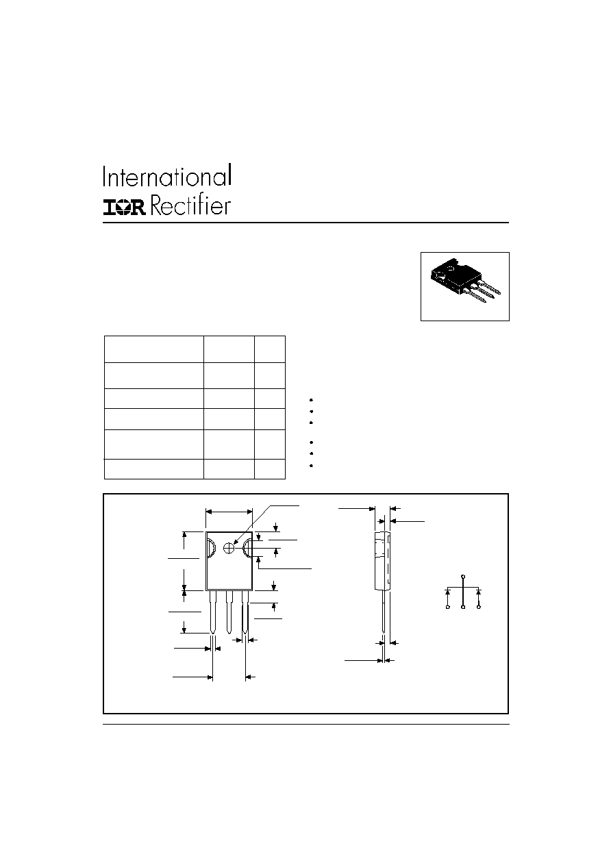
Dimensions in millimeters and inches
Conform to JEDEC outline TO-247AC (TO-3P)
2
BASE
COMMON
CATHODE
1
2
3
ANODE
COMMON
CATHODE
ANODE
1
2
TO-247AC
I
F(AV)
Rectangular
50
A
waveform
V
RRM
30
V
I
FSM
@ tp = 5 µs sine
2180
A
V
F
@
25 Apk, T
J
= 125°C
0.38
V
(per leg)
T
J
range
- 55 to 150
°C
SCHOTTKY RECTIFIER
50 Amp
52CPQ030
Bulletin PD-20556 rev. B 05/02
1
www.irf.com
52CPQ030
www.irf.com
Bulletin PD-20556 rev. B 05/02
2
Part number
52CPQ030
V
R
Max. DC Reverse Voltage (V)
V
RWM
Max. Working Peak Reverse Voltage (V)
Voltage Ratings
30
V
FM
Max. Forward Voltage Drop
0.48
V
@ 25A
(Per Leg) * See Fig. 1
(1)
0.55
V
@ 50A
0.38
V
@ 25A
0.49
V
@ 50A
I
RM
Max. Reverse Leakage Current
1.9
mA
T
J
= 25 °C
(Per Leg) * See Fig. 2
(1)
450
mA
T
J
= 125 °C
V
F(TO)
Threshold Voltage
0.24
V
T
J
= T
J
max.
r
t
Forward Slope Resistance
5.05
m
C
T
Max. Junction Capacitance (Per Leg)
4600
pF
V
R
= 5V
DC
, (test signal range 100Khz to 1Mhz) 25°C
L
S
Typical Series Inductance (Per Leg)
7.5
nH
Measured lead to lead 5mm from package body
dv/dt Max. Voltage Rate of Change
10000
V/ µs
(Rated V
R
)
T
J
Max. Junction Temperature Range
-55 to 150
°C
T
stg
Max. Storage Temperature Range
-55 to 150
°C
R
thJC
Max. Thermal Resistance Junction
0.8
°C/W DC operation
to Case (Per Leg) * See Fig. 4
R
thJC
Max. Thermal Resistance Junction
0.4
°C/W DC operation
to Case (Per Package)
R
thCS
Typical Thermal Resistance, Case
0.25
°C/W Mounting surface , smooth and greased
to Heatsink
wt
Approximate Weight
6 (0.21)
g (oz.)
T
Mounting Torque
Min.
6 (5)
Max.
12 (10)
Case Style
TO-247AC(TO-3P) JEDEC
Thermal-Mechanical Specifications
Kg-cm
(Ibf-in)
T
J
= 25 °C
T
J
= 125 °C
Electrical Specifications
(1) Pulse Width < 300µs, Duty Cycle <2%
V
R
= rated V
R
Absolute Maximum Ratings
Following any rated
load condition and with
rated V
RRM
applied
Parameters
52CPQ Units
Conditions
I
F(AV)
Max. Average Forward
(Per Leg)
25
A
50% duty cycle @ T
C
= 132°C, rectangular wave form
Current
* See Fig. 5
(Per Device)
50
I
FSM
Max. Peak One Cycle Non-Repetitive
2180
5µs Sine or 3µs Rect. pulse
Surge Current (Per Leg) * See Fig. 7
600
10ms Sine or 6ms Rect. pulse
E
AS
Non-Repetitive Avalanche Energy
27
mJ
T
J
= 25 °C, I
AS
= 6 Amps, L = 1.5 mH
(Per Leg)
I
AR
Repetitive Avalanche Current
6
A
Current decaying linearly to zero in 1 µsec
(Per Leg)
Frequency limited by T
J
max. V
A
= 1.5 x V
R
typical
A
Parameters
52CPQ Units
Conditions
Parameters
52CPQ Units
Conditions
52CPQ030
Bulletin PD-20556 rev. B 05/02
www.irf.com
3
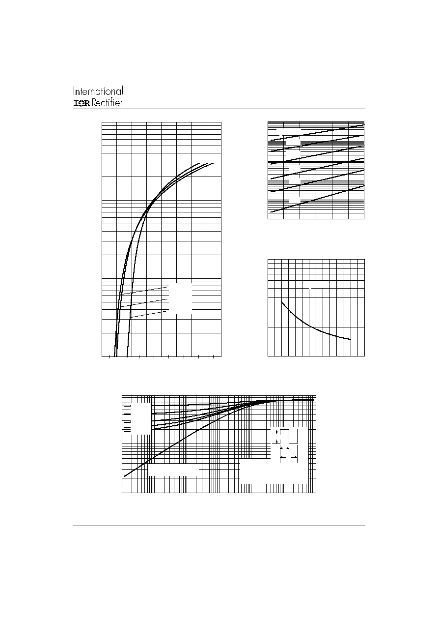
Fig. 2 - Typical Values Of Reverse Current
Vs. Reverse Voltage (Per Leg)
Fig. 3 - Typical Junction Capacitance
Vs. Reverse Voltage (Per Leg)
Fig. 4 - Max. Thermal Impedance Z
thJC
Characteristics (Per Leg)
Fig. 1 - Max. Forward Voltage Drop Characteristics
(Per Leg)
1
1 0
10 0
1 0 00
0
0.2
0 .4
0 .6
0 .8
1
1 .2
1.4
1.6
I
n
st
a
n
t
a
n
e
o
u
s F
o
rw
a
r
d C
u
r
r
e
n
t
-
I
(A
)
T = 150 C
T = 125 C
T = 25 C
J
J
J
F
F M
Forw ard V oltag e D rop - V (V )
0.0 1
0 .1
1
10
1 00
10 0 0
0
5
1 0
15
20
25
30
R
R
125 C
100 C
75 C
50 C
25 C
Re
v
e
r
s
e C
u
r
r
en
t
-
I
(
m
A
)
Re verse V olta g e - V (V)
T = 150 C
J
10 0 0
1 0 00 0
0
5
1 0
15
20
25
30
3 5
R
T
Ju
nc
t
i
on C
a
p
a
c
i
t
a
nc
e -
C
(
p
F
)
Re verse V olta g e - V (V )
T = 2 5 C
J
0 .0 1
0 .1
1
0 . 0 00 0 1
0 .0 0 0 1
0 .0 0 1
0 .0 1
0 .1
1
1 0
th
J
C
Sin gle P u lse
(Th erm a l Resista nc e)
1
T
h
e
r
m
a
l
I
m
p
e
d
a
n
c
e
Z
(
C
/
W
)
t , R ec tang ular Pulse D ura tio n (Sec o nd s)
D = 0.7 5
D = 0.5 0
D = 0.3 3
D = 0.2 5
D = 0.20
2
t
1
t
P
D M
1
2
J
D M
thJ C
C
N o te s:
1. D uty fa c to r D = t / t
2. P e a k T = P x Z + T
52CPQ030
www.irf.com
Bulletin PD-20556 rev. B 05/02
4
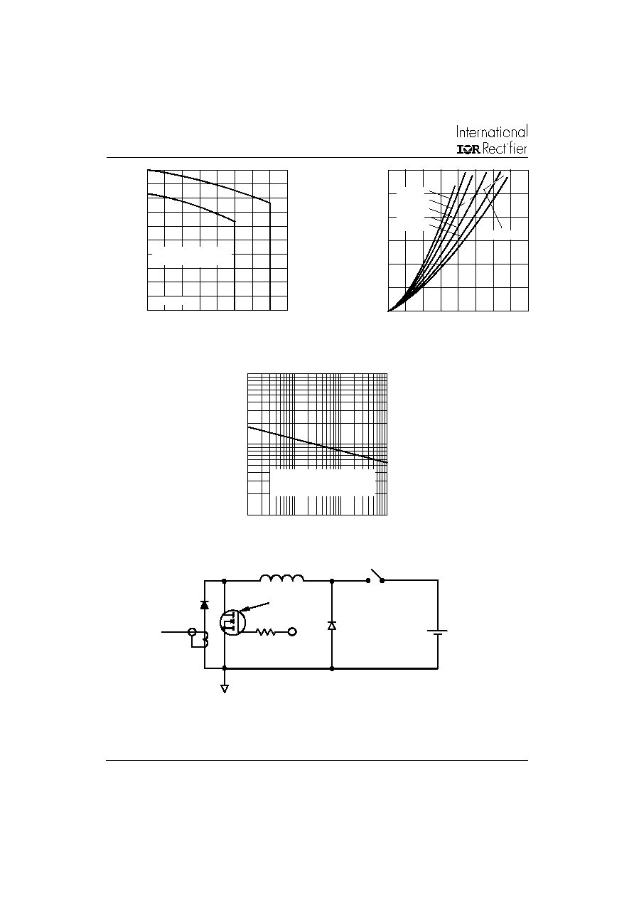
Fig. 7 - Max. Non-Repetitive Surge Current (Per Leg)
Fig. 5 - Max. Allowable Case Temperature
Vs. Average Forward Current (Per Leg)
Fig. 8 - Unclamped Inductive Test Circuit
Fig. 6 - Forward Power Loss Characteristics
(Per Leg)
FR EE-W HE EL
D IO D E
40H FL40S02
C UR RE N T
M O N ITO R
H IG H -SPE ED
SW ITC H
IRFP460
L
D UT
Rg = 25 ohm
V d = 25 V olt
+
(2) Formula used: T
C
= T
J
- (Pd + Pd
REV
) x R
thJC
;
Pd = Forward Power Loss = I
F(AV)
x V
FM
@ (I
F(AV)
/
D) (see Fig. 6);
Pd
REV
= Inverse Power Loss = V
R1
x I
R
(1 - D); I
R
@ V
R1
= 80% rated V
R
0
5
1 0
1 5
0
5
10
1 5
2 0
2 5
3 0
35
4 0
D C
Av
e
r
a
g
e
P
o
w
e
r
L
o
s
s
-
(
W
a
t
t
s
)
F(A V )
RM S Lim it
D = 0.20
D = 0.25
D = 0.33
D = 0.50
D = 0.75
A ve ra g e Forw a rd C urre n t - I (A)
1 00
1 10
1 20
1 30
1 40
1 50
0
5
1 0
1 5
2 0
25
30
3 5
40
D C
A
l
l
o
w
a
b
l
e C
a
s
e
T
e
m
p
er
a
t
ur
e
-
(
C
)
F(A V)
se e n o te ( 2)
Squa re w ave (D = 0.50)
80% Ra te d V ap p lie d
R
A ve rag e Forw a rd C urre n t - I (A )
100
1000
10000
10
100
1000
10000
FS
M
N
o
n
-
R
e
p
e
ti
t
i
v
e
S
u
r
g
e
C
u
r
r
e
n
t
-
I
(
A
)
p
At Any Rate d Load C ondition
An d W ith Rated V Applied
Follow in g Surg e
RRM
Square W ave Pulse D uration - t (m icrose c )
52CPQ030
Bulletin PD-20556 rev. B 05/02
www.irf.com
5
IR WORLD HEADQUARTERS: 233 Kansas St., El Segundo, California 90245, USA Tel: (310) 252-7105
TAC Fax: (310) 252-7309
Visit us at www.irf.com for sales contact information. 05/02
Data and specifications subject to change without notice.
This product has been designed and qualified for Industrial Level.
Qualification Standards can be found on IR's Web site.
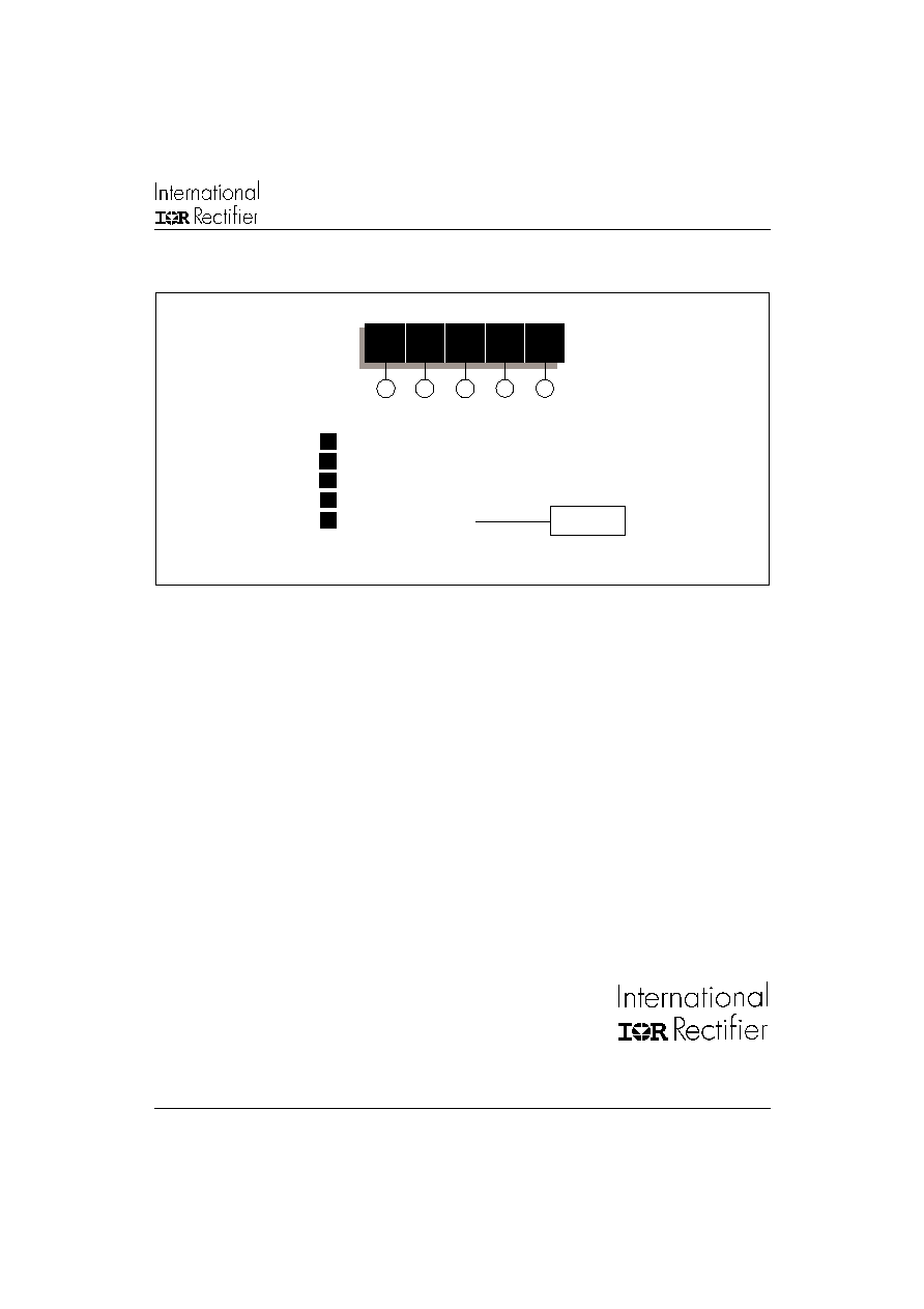
Ordering Information Table
Device Code
1
5
2
4
3
1
-
Essential Part Number
2
-
Common Cathode
3
-
P = TO-247
4
-
Q = Schottky Q Series
5
-
Voltage Rating
52
C
P
Q
030
030 = 30V
Standard Pack Quantity: 25 pcs