Äîêóìåíòàöèÿ è îïèñàíèÿ www.docs.chipfind.ru
10/24/02
www.irf.com
1
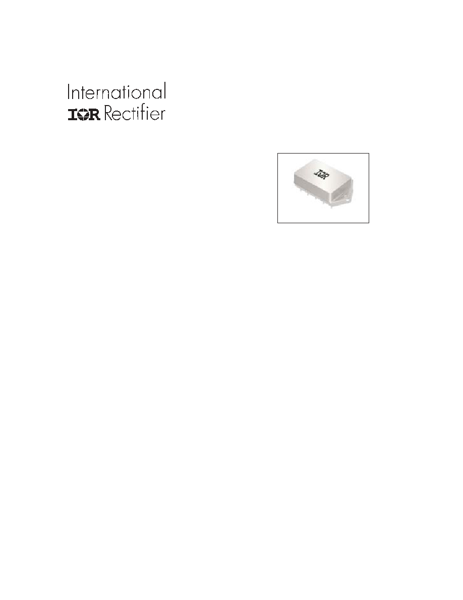
ADVANCED ANALOG
HYBRID-HIGH RELIABILITY
DC/DC CONVERTERS
ATW28XXD SERIES
Description
n
18 to 40 VDC Input Range (28 VDC Nominal)
n
±
12V and
±
15V Outputs Available
n
Indefinite Short Circuit and Overload
Protection
n
22.8 W/in
3
Power Density
n
30 W
Output Power
n
Fast Loop Response for Superior Transient
Characteristics
n
Operating Temperature Range from -55°C to
+125°C Available
n
Popular Industry Standard Pin-Out
n
Resistance Seam Welded Case for Superior
Long Term Hermeticity
n
Efficiencies up to 85%
n
Shutdown from External Signal
n
Full Military Screening
n
200,000 hour MTBF at 85°C
Features
ATW
28V Input, Dual Output
The advanced feedback design provides fast loop re-
sponse for superior line and load transient character-
istics and offers greater reliability and radiation toler-
ance than devices incorporating optical elements in
the feedback circuits.
Manufactured in a facility fully qualified to MIL-PRF-
38534, these converters are available in four screen-
ing grades to satisfy a wide range of requirements. The
CH grade is fully compliant to the requirements of MIL-
PRF-38534 for class H. The HB grade is processed
and screened to the class H requirement, but may not
necessarily meet all of the other MIL-PRF-38534 re-
quirements, e.g., element evaluation and Periodic In-
spection (PI) not required. Both grades are tested to
meet the complete group "A" test specification over the
full military temperature range without output power
deration. Two grades with a more limited screening
are also available for use in less demanding applica-
tions. Variations in electrical, mechanical and screen-
ing can be accommodated. Contact Advanced Analog
for special requirements.
n
MIL-PRF-38534 Compliant Versions
Available
Three standard temperature grades are offered. Refer
to Part Number section for more severe environments.
The ATW28XXD Series of DC/DC converters feature
high power density and an extended temperature range
for use in military and industrial applications. Designed
to MIL-STD-704 input requirements, these devices op-
erate with a nominal 28 VDC inputs with ±12V and ±15V
dual outputs to satisfy a wide range of requirements.
The circuit design incorporates a pulse width modu-
lated push-pull topology operating in the feed-forward
mode at a nominal switching frequency of 270KHz. Input
to output isolation is achieved through the use of trans-
formers in the forward and feedback circuits.
PD - 94557
2
www.irf.com
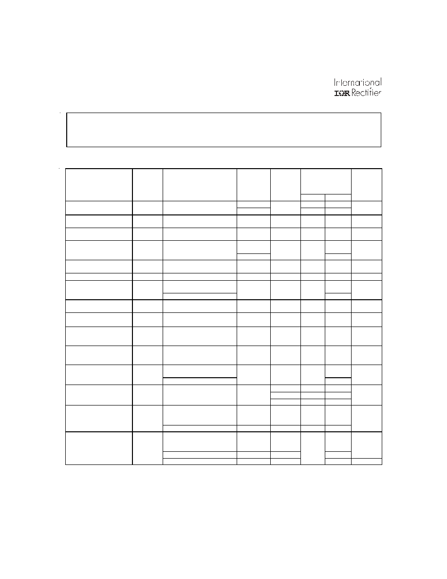
ATW28XXD Series
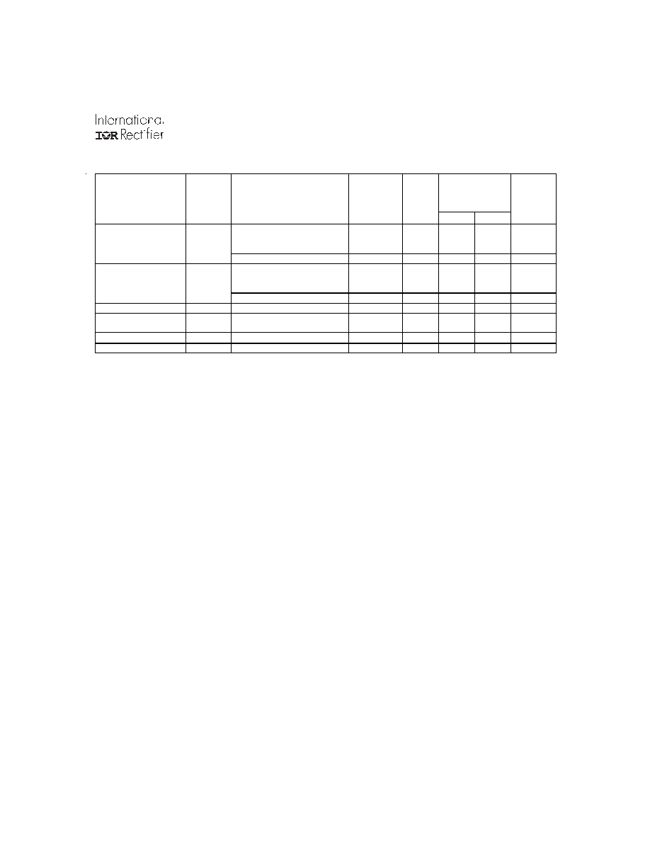
Specifications
For Notes to Specifications, refer to page 3
Table I. Electrical Performance Characteristics
ATW2812D
Test Symbol
Conditions
-55°C
Tc
+125°C
Vin = 28 Vdc ±5%, C
L
= 0
Unless otherwise specified
Group A
Subgroups
Device
Types
Limits Unit
Min
Max
Output voltage
V
OUT
I
OUT
= 0
1
All
±
11.88
±
12.12
V
2,3
±
11.76
±
12.24
Output current
1, 2
I
OUT
V
IN
= 18, 28, and 40 V dc,
each output
1,2,3 All
250
2250
mA
Output ripple voltage
3
V
RIP
V
IN
= 18, 28, and 40 V dc,
B.W. = 20Hz to 2MHz
1,2,3 All 85
mVp-p
Line regulation
4
VR
LINE
V
IN
= 18, 28, and 40 V dc,
Iout = 0,1250, and 2500mA
1 All
30
mV
2,3
60
Load regulation
4
VR
LOAD
V
IN
= 18, 28, and 40 V dc,
I
OUT
= 0, 1250, and 2500mA
1,2,3 All 120
mV
Cross regulation
5
VR
CROSS
10% to 90% load change
1,2,3
All
3.5
%
Input current
I
IN
I
OUT
= 0, inhibit (pin 8)
tied to input return (pin 10)
1,2,3 All 18 mA
I
OUT
= 0,inhibit (pin 8)= open
50
Input ripple current
3, 4
I
RIP
I
OUT
= 2500mA
B.W. = 20Hz to 2MHz
1,2,3 All 50
mAp-p
Efficiency
4
E
FF
I
OUT
= 2500mA
1
All
80
%
T
C
= +25
°
C
Isolation
ISO
Input to output or any pin
to case (except pin 7) at
500 V dc Tc = +25°C
1 All
100
M
Capacitive load
6, 7
C
L
No effect on dc
performance, Tc = +25°C,
total for both outputs
4 All
200
µF
Power dissipation
load fault
P
D
Overload, T
C
= +25
°
C
8
1 All
12
W
Short circuit, T
C
= +25
°
C
9
Switching frequency
4
F
S
I
OUT
= 2500mA
4,5,6
01
250
300
KHz
02
250
270
03
275
300
Output response to step
transient load
changes
4, 9
VO
TLOAD
1250mA to/from 2500mA
4,5,6
All
-400
+400
mV pk
0mA to/from 2500mA
4,5,6
All
-800
+800
Recovery time step
transient load
changes
4, 9, 10
TT
LOAD
1250mA to/from 2500mA
4,5,6
All
70
µs
0mA to/from 1250mA
4,5,6
All
500
1250mA to/from 0mA
4,5,6
All
5
ms
Input Voltage -0.5V to 50V
Soldering Temperature 300°C for 10 seconds
Case Temperature Operating -55°C to +125°C
Storage -65°C to +135°C
ABSOLUTE MAXIMUM RATINGS
www.irf.com
3
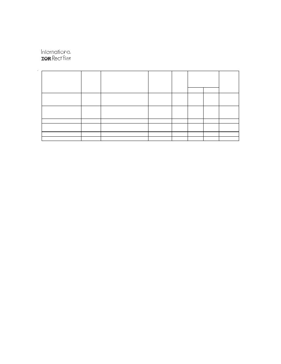
ATW28XXD Series
Notes to Specifications
Table I. Electrical Performance Characteristics -
continued
ATW2812D
1 Parameter guaranteed by line, load and cross regulation tests.
2 Up to 90% of full power is available from either output provided the total output does not exceed 30W.
3 Bandwidth guaranteed by design. Tested for 20KHz to 2MHz.
4 Load current split equally between +V
OUT
and V
OUT
.
5 Three-watt load on output under test, 3 watt to 27 watt load change on other output.
6 Capacitive load may be any value from 0 to the maximum limit without compromising dc performance.
A capacitive load in excess of the maximum limit will not disturb loop stability but may interfere with the
operation of the load fault detection circuitry, appearing as a short circuit during turn-on.
7 Parameter shall be tested as part of design characterization and after design or process changes.
Thereafter, parameters shall be guaranteed to the limits specified in Table I.
8 An overload is that condition with a load in excess of the rated load but less than that necessary to
trigger the short circuit protection and is the condition of maximum power dissipation.
9 Load step transition time between 2 and 10 microseconds.
10 Recovery time is measured from the initiation of the transient to where V
OUT
has returned to within ±1
percent of V
OUT
at 50 percent load.
11 Input step transition time between 2 and 10 microseconds.
12 Turn-on delay time measurement is for either a step application of power at the input or the removal of
ground signal from the inhibit pin (pin 8) while power is applied to the input.
Test Symbol Conditions
-55°C
Tc
+125°C
Vin = 28 Vdc ±5%, C
L
= 0
unless otherwise specified
Group A
Subgroups
Device
Types
Limits Unit
Min
Max
Output response
transient step line
changes
4, 7, 11
VO
TLINE
Input step from/to 18 to 40
Vdc, I
OUT
= 2500mA
4,5,6 All
-800
+800
mV
pk
Recovery time
transient step line
change
4, 7, 10, 11
TT
LINE
Input step from/to 18 to 40
Vdc, I
OUT
= 2500mA
4,5,6 All
4000
µ
s
Turn on overshoot
4
VTon
OS
I
OUT
=
0 and 2500mA
4,5,6
All
750
mV pk
Turn on delay
4, 12
Ton
D
I
OUT
= 0 and 2500mA
4,5,6 All 14 ms
Load fault recovery
7
Tr
LF
4,5,6 All 14 ms
Weight
Flange
75
grams
4
www.irf.com
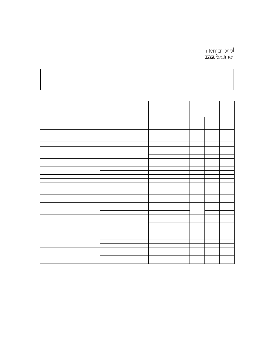
ATW28XXD Series
Specifications
Table II. Electrical Performance Characteristics
ATW2815D
For Notes to Specifications, refer to page 5
Test Symbol Conditions
-55°C
Tc
+125°C
Vin = 28 Vdc ±5%, C
L
= 0
Unless otherwise specified
Group A
Subgroups
Device
Types
Limits Unit
Min
Max
Output voltage
V
OUT
V
IN
= 18, 28, and 40 Vdc
1
All
±
14.85
±
15.15
V
DC
I
OUT
= 0
2,3
All
±
14.70
±
15.30
V
DC
Output current
11, 13
I
OUT
V
IN
= 18, 28, and 40 V dc
1,2,3
All
0.200
2000
mA
DC
Output ripple voltage
8
V
RIP
V
IN
= 18, 28, and 40 V dc,
B.W. = DC to MHz
1,2,3 All
85
mVp-p
Output Power
4, 11
P
OUT
V
IN
= 18, 28, 40 Vdc
1,2,3
All
30
W
Line regulation
9, 10
VR
LINE
V
IN
= 18, 28, and 40 V dc,
Iout = 0, 1000, and 2000mA
1 All
35
mV
2,3
All
75
mV
Load regulation
9, 10
VR
LOAD
V
IN
= 18, 28, and 40 V dc,
I
OUT
= 0, 1000, and 2000mA
1,2,3 All
150
mV
Input current
I
IN
I
OUT
= 0, inhibit (pin 8)
1,2,3
All
12
mADC
I
OUT
= 0, inhibit (pin 8) = open
1,2,3
All
30
mADC
Input ripple current
I
RIP
I
OUT
= 2000mA
1,2,3
All
60
mAp-p
Efficiency
E
FF
I
OUT
= 2500mA T
C
= 25
°
C
1
All 80 %
Isolation
ISO
Input to output or any pin
to case (except pin 8) at
500V dc Tc = 25°C
1 All
100
M
Capacitive load
6, 12
C
L
No effect on dc performance,
Tc = 25°C
4 All
500
µF
Power dissipation
load fault
P
D
Overload, T
C
= +25
°
C
3
1 All
9
W
Short circuit, T
C
= +25
°
C
1 All
9
W
Switching frequency
F
S
I
OUT
= 2000mA
1,2,3
01
237
263
KHz
1,2,3
02
230
245
KHz
1,2,3
03
250
265
KHz
Output response to step
transient
load changes
7, 9, 10
VO
TLOAD
50% load to/from 100% load
4,5,6
All
-300
+300
mV pk
No load to 100% load
4,5,6
All
-800
-800
mV pk
100% load to no load
4,5,6
All
+800
+800
mV pk
Recovery time step
transient load changes
1, 7
TT
LOAD
50% load to/from 100% load
4,5,6
All
25
µs
No load to 50% load
4,5,6
All
500
µs
50% load to no load
4,5,6
All
7
ms
Input Voltage -0.5V to 50V
Soldering Temperature 300°C for 10 seconds
Case Temperature Operating -55°C to +125°C
Storage -65°C to +135°C
ABSOLUTE MAXIMUM RATINGS
www.irf.com
5
ATW28XXD Series
Table II. Electrical Performance Characteristics -
continued
Notes to Specifications
ATW2815D
1 Recovery time is measured from the initiation of the transient to where V
OUT
has returned to within
±
1% of V
OUT
at 50% load.
2 Turn-on delay time measurement is for either a step application of power at the input or the removal of a ground signal from the
inhibit pin (pin 8) while power is applied to the input.
3 An overload is that condition with a load in excess of the rated load but less than that necessary to trigger the short circuit
protection and is the condition of maximum power dissipation.
4 Above +125
°
C case, derate output power linearly to 0 at +135
°
C case.
5 Input step transition time between 2 and 10 microseconds.
6 Capacitive load may be any value from 0 to the maximum limit without compromising DC performance. A capacitive load in
excess of the maximum limit will not disturb loop stability but will interfere with the operation of the load fault detection circuitry,
appearing as a short circuit during turn on.
7 Load step transition time between 2 and 10 microseconds.
8 Bandwidth guaranteed by design. Tested for 20KHz to 2MHz.
9 Load current split equally between +V
OUT
and V
OUT
.
10 When operating with unbalanced loads, at least 25% of the load must be on the positive output to maintain regulation.
11 Parameter guaranteed by line and load regulation tests.
12 Parameter shall be tested as part of design characterization and after design or process changes. Thereafter parameters shall be
guaranteed to the limits specified in Table II.
13 Up to 90% of full power is available from either output provided the total output does not exceed 30 watts.
Test Symbol Conditions
-55°C
Tc
+125°C
Vin = 28 Vdc ±5%, C
L
= 0
unless otherwise specified
Group A
Subgroups
Device
Types
Limits Unit
Min
Max
Output response
transient step line
changes
5, 12
VO
TLINE
Input step from/to 18 to
40VDC
4,5,6 All
+180
mV
pk
Input step from 40 to18 VDC
4,5,6
All
-600
mV pk
Recovery time
transient step line
changes
1. 5, 12
TT
LINE
Input step from/to 18 to 40
VDC
4,5,6 All 400
µ
s
Input step from 40 to 18 VDC
4,5,6
All
400
µ
s
Turn on overshoot
VTon
OS
I
OUT
=
0 and 2000mA
4,5,6
All
750
mV pk
Turn on delay
2
Ton
D
I
OUT
= 0 and 2000mA
4,5,6 All 12 ms
Load fault recovery
12
Tr
LF
V
IN
= 18 to 40 VDC
4,5,6
All
12
ms
Weight
Flange
75
grams