 | –≠–ª–µ–∫—Ç—Ä–æ–Ω–Ω—ã–π –∫–æ–º–ø–æ–Ω–µ–Ω—Ç: 80SCLQ030 | –°–∫–∞—á–∞—Ç—å:  PDF PDF  ZIP ZIP |
SCHOTTKY RECTIFIER
80 Amp, 30V
80SCLQ030
Major Ratings and Characteristics
Description/Features
7/11/01
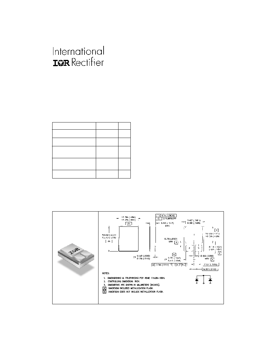
CASE STYLE
IR Case Style SMD-1
www.irf.com
1
Characteristics
80SCLQ030 Units
I
F(AV)
80
A
V
RRM
(Per Leg)
30
V
I
FSM
@ tp = 8.3ms half-sine
(Per Leg)
200
A
V
F
@ 40Apk, T
J
=125∞C
0.55
V
(Per Leg)
T
J
, T
stg
Operating and storage
-55 to 150
∞C
ANODE COMMON ANODE
CATHODE
2
1
3
HIGH EFFICIENCY SERIES
The 80SCLQ030 center tap Schottky rectifier has been
expressly designed to meet the rigorous requirements of hi-
rel environments. It is packaged in the hermetic surface
mount SMD-1 ceramic package. The device's forward
voltage drop and reverse leakage current are optimized for
the lowest power loss and the highest circuit efficiency for
typical high frequency switching power supplies and
resonent power converters. Full MIL-PRF-19500 quality
conformance testing is available on source control drawings
to TX, TXV and S quality levels.
∑ Hermetically Sealed
∑ Center Tap
∑ Low Forward Voltage Drop
∑ High Frequency Operation
∑ Guard Ring for Enhanced Ruggedness and Long term
Reliability
∑ Surface Mount
∑ Lightweight
PD -94188A

80SCLQ030
2
www.irf.com
Part number
80SCLQ030
V
R
Max. DC Reverse Voltage (V) (Per Leg)
V
RWM
Max. Working Peak Reverse Voltage (V) (Per Leg)
Voltage Ratings
30
Parameters
Limits Units
Conditions
I
F(AV)
Max. Average Forward Current
80
A
50% duty cycle @ T
C
= 81∞C, square waveform
See Fig. 5
I
FSM
Max. Peak One Cycle Non - Repetitive
200
A
@ t
p
= 8.3 ms half-sine
Surge Current (Per Leg)
Absolute Maximum Ratings
Parameters
Limits
Units
Conditions
V
FM
Max. Forward Voltage Drop
0.58
V
@ 20A
(Per Leg) See Fig. 1
Q
0.7
V
@ 40A
T
J
= -55∞C
R
0.83
V
@ 80A
0.47
V
@ 20A
0.56
V
@ 40A
T
J
= 25∞C
R
0.73
V
@ 80A
0.42
V
@ 20A
0.55
V
@ 40A
T
J
= 125∞C
R
0.82
V
@ 80A
I
RM
Max. Reverse Leakage Current
1.5
mA
T
J
= 25∞C
(Per Leg) See Fig. 2
Q
75
mA
T
J
= 100∞C
V
R
= rated V
R
R
200
mA
T
J
= 125∞C
C
T
Max. Junction Capacitance (Per Leg)
2600
pF
V
R
= 5V
DC
( 1MHz, 25∞C )
R
L
S
Typical Series Inductance (Per Leg)
5.9
nH
Measured from center of cathode pad to center of
anode pad
Electrical Specifications
Q
Pulse Width < 300µs, Duty Cycle < 2%
Parameters
Limits
Units
Conditions
T
J
Max.Junction Temperature Range
-55 to 150
∞C
T
stg
Max. Storage Temperature Range
-55 to 150
∞C
R
thJC
Max. Thermal Resistance, Junction
1.25
∞C/W
DC operation
See Fig. 4
to Case (Per Leg)
R
thJC
Max. Thermal Resistance, Junction
0.63
∞C/W
DC operation
to Case (Per Package)
wt
Weight (Typical)
2.6 g
Die Size (Typical)
150X180 mils
Thermal-Mechanical Specifications
Case Style
SMD-1

80SCLQ030
www.irf.com
3
Fig. 2 - Typical Values of Reverse Current
Vs. Reverse Voltage (Per Leg)
Fig. 3 - Typical Junction Capacitance Vs.
Reverse Voltage (Per Leg)
Fig. 1 - Max. Forward Voltage Drop Characteristics
(Per Leg)
0
10
20
30
Reverse Voltage -VR (V)
1000
10000
Junction Capacitance - C
T
(pF)
TJ = 25∞C
0
10
20
30
Reverse Voltage - VR (V)
0.01
0.1
1
10
100
1000
Reverse Current - I
R
( mA )
125∞C
75∞C
25∞C
100∞C
0.0
0.2
0.4
0.6
0.8
1.0
Forward Voltage Drop - V F (V)
1
10
100
Instantaneous Forward Current - I
F
(A)
Tj = -55∞C
Tj = 125∞C
Tj = 25∞C

80SCLQ030
4
www.irf.com
Fig. 5 - Max. Allowable Case Temperature Vs.
Average Forward Current
Fig. 4 - Max. Thermal Impedance Z
thJC
Characteristics (Per Leg)
IR WORLD HEADQUARTERS: 233 Kansas St., El Segundo, California 90245, USA Tel: (310) 252-7105
TAC Fax: (310) 252-7903
Visit us at www.irf.com for sales contact information.
Data and specifications subject to change without notice. 07/01
0.01
0.1
1
10
0.00001
0.0001
0.001
0.01
0.1
1
Notes:
1. Duty factor D = t / t
2. Peak T = P
x Z
+ T
1
2
J
DM
thJC
C
P
t
t
DM
1
2
t , Rectangular Pulse Duration (sec)
Thermal Response
(Z )
1
thJC
0.01
0.02
0.05
0.10
0.20
D = 0.50
SINGLE PULSE
(THERMAL RESPONSE)
0
20
40
60
80
100
120
Average Forward Current - I F(AV) (A)
0
20
40
60
80
100
120
140
160
180
Allowable Case Temprature - (
∞
C)
80SCLQ030
R thJC = 0.63∞C/W
DC