 | –≠–ª–µ–∫—Ç—Ä–æ–Ω–Ω—ã–π –∫–æ–º–ø–æ–Ω–µ–Ω—Ç: F6456S | –°–∫–∞—á–∞—Ç—å:  PDF PDF  ZIP ZIP |

www.irf.com
IRIS-F6456S
Features
∑ Oscillator is provided on the monolithic control with adopting On-Chip-
Trimming technology.
∑ Small temperature characteristics variation by adopting a comparator to
compensate for temperature on the control part.
∑ Low start-up circuit current (100uA max)
∑ Built-in Active Low-Pass Filter for stabilizing the operation in case of light
load
∑ Avalanche energy guaranteed MOSFET with high VDSS
∑ The built-in power MOSFET simplifies the surge absorption circuit
since the MOSFET guarantees the avalanche energy.
∑ No VDSS de-rating is required.
∑ Built-in constant voltage drive circuit
∑ Built-in soft drive circuit
∑ Built-in low frequency PRC mode (20kHz)
∑ Various kinds of protection functions
∑ Pulse-by-pulse Overcurrent Protection (OCP)
∑ Overvoltage Protection with latch mode (OVP)
∑ Thermal Shutdown with latch mode (TSD)
INTEGRATED SWITCHER
Package Outline
TO-247 Fullpack (5 Lead)
Descriptions
IRIS-F6456S is a hybrid IC consists from power MOSFET and a controller IC, designed for Quasi-Resonant (including
low frequency PRC) fly-back converter type SMPS (Switching Mode Power Supply) applications. This IC realizes
high efficiency, low noise, downsizing and standardizing of a power supply system reducing external components count
and simplifying the circuit designs. (Note). PRC is abbreviation of "Pulse Ratio Control" (On-width control with fixed
OFF-time).
Typical Connection Diagram
S
S
S
S
G
G
G
GNNNNDDDD
V
V
V
Viiiinnnn
D
D
D
D
O
O
O
OCCCCPPPP////FFFFBBBB
I
I
I
IRRRRIIIISSSS----FFFF6666444400000000
Type
MOSFET
VDSS(V)
RDS(ON)
MAX
AC input(V)
Pout(W)
Note 1
230±15%
300
85 to 264
150
IRIS-F6456S
650
0.71
Key Specifications
Data Sheet No. PD 96942A
Note 1: The Pout (W) represents the thermal rating at Quasi-Resonant
Operation, and the peak power output is obtained by approximately 120
to 140% of the above listed. When the output voltage is low and ON-
duty is narrow, the Pout (W) shall become lower than that of above.

www.irf.com
*1 Refer to MOS FET A.S.O curve
*2 MOS FET Tch-EAS curve
*3 Refer to MOS FET Ta-PD1 curve
*4 Refer to TF-PD2 curve for Control IC (See page 5)
*5 Maximum switching current.
The maximum switching current is the Drain current determined by the drive voltage of the IC and
threshold voltage (Vth) of MOS FET. Therefore, in the event that voltage drop occurs between Pin 2 and
Pin 5 due to patterning, the maximum switching current decreases as shown by V
2-5
in Fig.1
Accordingly please use this device within the decrease value, referring to the derating curve of the
maximum switching current.
Absolute Maximum Ratings (Ta=25∫C)
Absolute maximum ratings indicate sustained limits beyond which damage to the device may occur. All voltage parameters are
absolute voltages referenced to terminals stated, all currents are defined positive into any lead. The thermal resistance and power
dissipation ratings are measured under board mounted and still air conditions.
Symbol
Definition
Terminals Max. Ratings
Units
Note
I
Dpeak
Drain Current *1
3-2
16
A
Single Pulse
V
2-5
=0.78V
Ta=-20~+125
I
L peak
=6.4A
Vin
Input voltage for control part
4-5
35
V
Vth
O.C.P/F.B Pin voltage
1-5
6
V
58
W
With infintite heatsink
2.8
W
Without heatsink
Power dissipation for control part
(Control IC) *4
Internal frame temperature
Refer to recommended
in operation
operating temperature
Top
Operating ambient temperature
-
-20 ~ +125
Tstg
Storage temperature
-
-40 ~ +125
Tch
Channel temperature
-
150
Single Pulse
P
D1
Power dissipation for MOSFET *3
3-2
A
Single pulse avalanche energy *2
3-2
E
AS
521
mJ
Maximum switching current *5
3-2
I
DMAX
16
Specified by
Vin◊Iin
-
T
F
-20 ~ +125
4-5
P
D2
0.49
W
V
2-5
Fig.1
IRIS-F6456S
Recommended operating conditions
Time for input of quasi resonant signals
For the quasi resonant signal inputted to O.C.P/F.B Pin
at the time of quasi resonant operation, the signal shall
be wider than T
th(2).
Vth(2)
O.C.P/F.B
Tth(2)1.0sec
0V
www.irf.com
Electrical Characteristics (for Control IC)
Electrical characteristics for control part (Ta=25, Vin=18V,unless otherwise specified)
MIN
TYP
MAX
V
in(ON)
Operation start voltage
14.4
16
17.6
V
Vin=017.6V
V
in(OFF)
Operation stop voltage
9
10
11
V
Vin=17.69V
I
in(ON)
Circuit current in operation
-
-
20
mA
-
I
in(OFF)
Circuit current in non-operation
-
-
100
µA
Vin=14V
T
OFF(MAX)
Maximum OFF time
45
-
55
µsec
-
Tth(2)
Minimum time for input of quasi
resonant signals *6
-
-
1
µsec
-
T
OFF(MIN)
Minimum OFF time *7
-
-
2
µsec
-
Vth(1)
O.C.P/F.B Pin threshold voltage 1
0.68
0.73
0.78
V
-
Vth(2)
O.C.P/F.B Pin threshold voltage 2
1.3
1.45
1.6
V
I
OCP/FB
O.C.P/F.B Pin extraction current
1.2
1.35
1.5
mA
-
V
in(OVP)
O.V.P operation voltage
20.5
22.5
24.5
V
Vin=024.5V
V
in(La.OFF)
Latch circuit release voltage *8
6.6
-
8.4
V
Vin=24.56.6V
Tj
(TSD)
Thermal shutdown operating temperature
140
-
-
Latch circuit sustaining current *8
Definition
Symbol
Vin=24.58.5V
Ratings
Units
Test
Conditions
I
in(H)
-
-
400
µA
Electrical Characteristics (for MOSFET)
*6 Refer to Recommended operating conditions (See page 2)
*7 The minimum OFF time means T
OFF
width at the time when the minimum quasi resonant signal is inputted.
*8 The latch circuit means a circuit operated O.V.P and T.S.D.
(Ta=25) unless otherwise specified
MIN
TYP
MAX
ID=300µA
V5
- 2
=0V(short)
V
DS
=650V
V5-2=0V(short)
V5-2=10V
I
D
=3.2A
tf
Switching time
-
-
250
nsec
-
Between channel and
internal frame
Ratings
Units
Test Conditions
Drain-to-Source breakdown voltage
V
Definition
V
DSS
650
-
-
Symbol
µA
On-resistance
R
DS(ON)
-
-
0.71
Drain leakage current
I
DSS
-
ch-F
-
-
Thermal resistance
300
-
0.85
/W
IRIS-F6456S

www.irf.com
IRIS-F6456S
MOSFETA.S.O. Curve
0.01
0.1
1
10
100
1
10
100
1000
Drain-to-Source Voltage V
DS
[V]
D
0.1ms
1ms
Drain current
limit by ON
resistance
ASO temperature derating
shall be made by obtaining
ASO Coefficient from the left
curve in your use.
IRIS-F6456S
IRIS-F6456S
A.S.O. temperature derating coefficient curve
0
20
40
60
80
100
0
20
40
60
80
100
120
Internal frame temperature TF []
A
.
S
.
O
.
tem
p
erature derating coefficient[%
]
IRIS-F6456S
Maximum Switching current derating curve
Ta=20+125
0.0
2.0
4.0
6.0
8.0
10.0
12.0
14.0
16.0
18.0
0.70
0.80
0.90
1.00
1.10
1.20
V
2-5
[V]
Maximum Switchng Current I
DMAX
[A]
IRIS-F6456S
A valanche energy derating curve
0
20
40
60
80
100
25
50
75
100
125
150
Channel temperature Tch [ ]
E
AS
tem
p
er
atur
e der
a
ting coef
f
i
cient [
%
]
Ta=25∫C
Single Pulse
Dr
ai
n Cu
rr
en
t I
D
[A
]

www.irf.com
IRIS-F6456S
Transient thermal resistance curve
0.001
0.01
0.1
1
10
tim e
t [sec]
Tr
an
s
i
en
t th
er
m
a
l r
e
s
i
s
t
an
ce
ch
-
c
[
/W
]
IRIS-F6456S
MIC T
F
-P
D2
Curve
0
0.1
0.2
0.3
0.4
0.5
0.6
0
20
40
60
80
100
120
140
160
Internal frame temperature T
F
[]
Pow
e
r di
ssi
pat
i
on P
D2
[W]
IRIS-F6456S
MOSFET Ta-P
D1
Curve
0
10
20
30
40
50
60
70
0
20
40
60
80
100 120 140 160
Ambient temperature Ta[]
Pow
e
r
di
ssi
pat
i
on P
D1
[W
]
1µ
10µ 100µ
1m
10m
100m
P
D2
=0.49[W]
P
D1
=58[W]
With infinite
heatsink
Without
heatsink
P
D1
=2.8[W]
IRIS-F6456S
www.irf.com
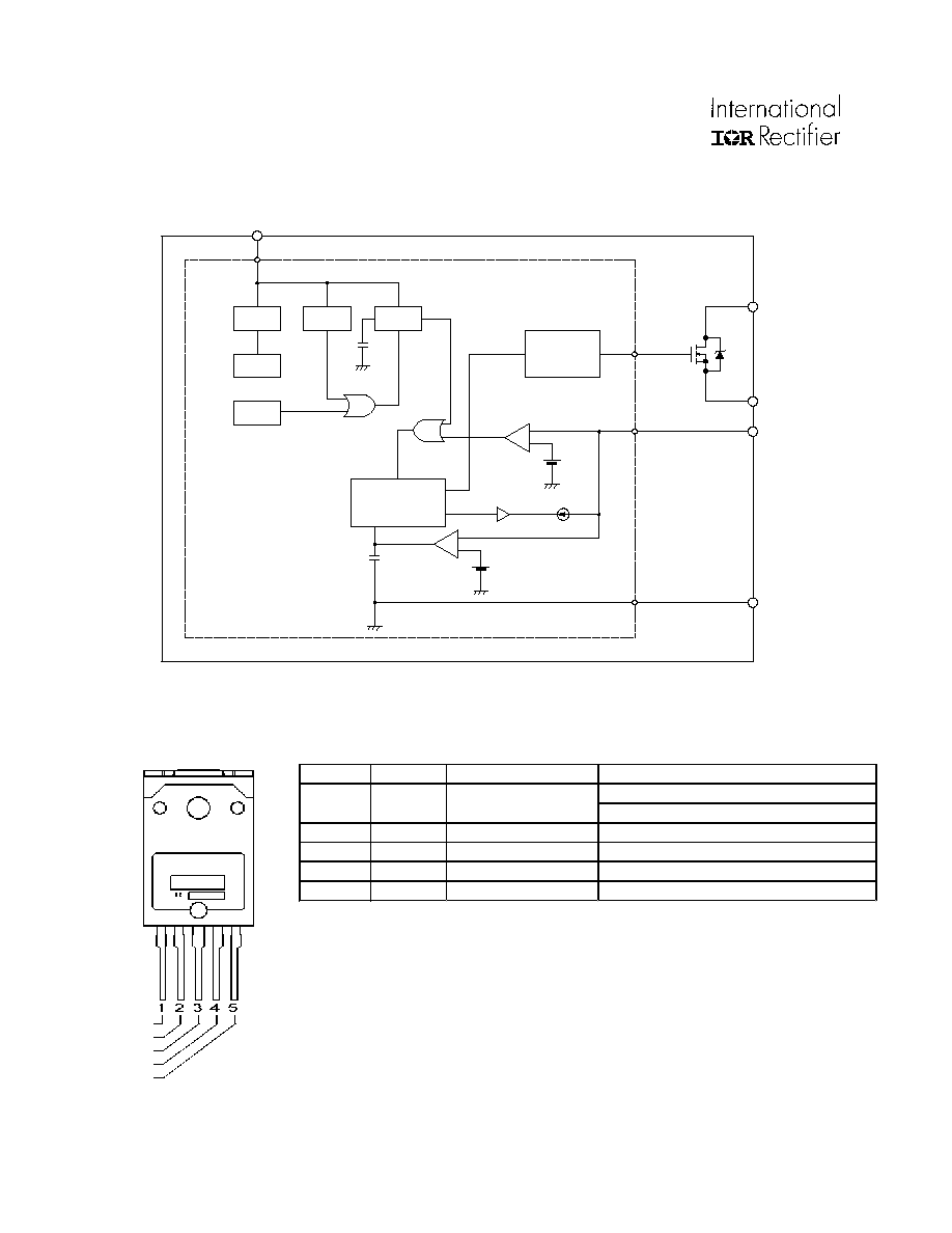
O.V.P.
+
-
+
-
START
LATCH
REG.
T.S.D
Vth(1)
Vth(2)
DRIVE
O.S.C
3
D
2
S
1
OCP/FB
5
GND
4 Vin
Pin No.
Symbol
Description
Function
Input of overcurrent detection
signal / constant voltage control signal
2
S
Source Pin
MOSFET source
3
D
Drain Pin
MOSFET drain
4
Vin
Power supply Pin
Input of power supply for control circuit
5
GND
Ground Pin
Ground
OCP/FB
Overcurrent / Feedback
Pin
1
Block Diagram
Lead Assignments
Other Functions
O.V.P. ≠ Overvoltage Protection Circuit
T.S.D. ≠ Thermal Shutdown Circuit
STEP DRV ≠ 2 step drive circuit
OCP/FB
S
D
Vin
GND
IRIS-F6456S
IRIS

www.irf.com
Data and specifications subject to change without notice.
IR WORLD HEADQUARTERS: 233 Kansas St., El Segundo, California 90245, USA Tel: (310) 252-7105
TAC FAX: (310) 252-7903
Visit us at www.irf.com for sales contact information.
Case Outline
0
0
0
0.
.
.
.5
5
5
5
0
0
0
0.
.
.
.5
5
5
5
5
5
5
5
4
4
4
4
3
3
3
3
2
2
2
2
1
1
1
1
±
±
±
±0000....2222
1
1
1
15
5
5
5.
.
.
.6
6
6
6
2
2
2
2-
-
-
-(
(
(
(R
R
R
R1
1
1
1.
.
.
.3
3
3
3)
)
)
)
R
R
R
R-
-
-
-e
e
e
en
n
n
nd
d
d
d
R
R
R
R-
-
-
-e
e
e
en
n
n
nd
d
d
d
(
(
(
(
4
4
4
4
)
)
)
)
±
±
±
±
0
0
0
0
.
.
.
.
5
5
5
5
7
7
7
7
±
±
±
±
0
0
0
0
.
.
.
.
5
5
5
5
3
3
3
3
.
.
.
.
3
3
3
3
±
±
±
±0000....7777
4
4
4
4.
.
.
.5
5
5
5
±
±
±
±0000....1111
3
3
3
3.
.
.
.3
3
3
35
5
5
5
-
-
-
-0
0
0
0.
.
.
.1
1
1
1
+
+
+
+0
0
0
0.
.
.
.2
2
2
2
0
0
0
0.
.
.
.6
6
6
65
5
5
5
±
±
±
±0000....2222
3
3
3
3.
.
.
.4
4
4
45
5
5
5
±
±
±
±0000....2222
5
5
5
5.
.
.
.5
5
5
5
I
I
I
IR
R
R
R
I
I
I
IR
R
R
RI
I
I
IS
S
S
S
-
-
-
-0
0
0
0.
.
.
.1
1
1
1
+
+
+
+0
0
0
0.
.
.
.2
2
2
2
1
1
1
1.
.
.
.3
3
3
35
5
5
5
±
±
±
±0000....2222
3333....2222
±
±
±
±
0
0
0
0
.
.
.
.
2
2
2
2
2
2
2
2
-
-
-
-0
0
0
0.
.
.
.1
1
1
1
+
+
+
+0
0
0
0.
.
.
.2
2
2
2
0
0
0
0.
.
.
.8
8
8
85
5
5
5
-
-
-
-0
0
0
0.
.
.
.1
1
1
1
+
+
+
+0
0
0
0.
.
.
.2
2
2
2
1
1
1
1.
.
.
.7
7
7
75
5
5
5
±
±
±
±
0
0
0
0
.
.
.
.
2
2
2
2
5
5
5
5
.
.
.
.
5
5
5
5
±
±
±
±
0
0
0
0
.
.
.
.
3
3
3
3
2
2
2
2
3
3
3
3
3
3
3
3
.
.
.
.
3
3
3
3
4
4
4
4xxxxPPPP2222....55554444±
±
±
±0000....1111====((((11110000....11116666))))
aType Number F6456S
bLot Number
1st letterThe last digit of year
2nd letterMonth
1 to 9 for Jan. to Sept.,
O for Oct. N for Nov. D for
Dec.
3rd & 4th letterDay
Arabic Numerals
5
th
letter : Registration Symbol
Weight : Approx. 7.5g
Dimensions in mm
DWG.No.4B-E01515A
Material of Pin : Cu
Treatment of Pin : Ni plating + solder dip
IRIS-F6456S
a
b