 | ÐлекÑÑоннÑй компоненÑ: HFA08SD60 | СкаÑаÑÑ:  PDF PDF  ZIP ZIP |
hfa08sd60s-revA
1
V
RRM
Cathode-to-Anode Voltage
600
V
I
F(AV)
Continuous Forward Current
8
A
T
C
= 100°C
I
FSM
Single Pulse Forward Current
60
I
FRM
Peak Repetitive Forward Current
24
P
D
Maximum Power Dissipation
14
W
T
C
= 100°C
T
J
,
T
STG
Operating Junction and Storage Temperatures
- 55 to 150
°C
Parameters
Max
Units
HFA08SD60S
Bulletin PD-20618 rev. B 07/02
t
rr
= 18ns
I
F(AV)
= 8Amp
V
R
= 600V
Features
Description/ Applications
Absolute Maximum Ratings
Ultrafast, Soft Recovery Diode
· Ultrafast Recovery Time
· Ultrasoft Recovery
· Very Low I
RRM
· Very Low Q
rr
· Guaranteed Avalanche
· Specified at Operating Temperature
D - PAK
Package Outline
These diodes are optimized to reduce losses and EMI/RFI in
high frequency power conditioning systems. The softness of
the recovery eliminates the need for a snubber in most
applications. These devices are ideally suited for freewheeling,
flyback, power converters, motor drives, and other applications
where high speed and reduced switching losses are design
requirements.
Benefits
· Reduced RFI and EMI
· Reduced Power Loss in Diode and
Switching Transistor
· Higher Frequency Operation
· Reduced Snubbing
· Reduced Parts Count
www.irf.com
HFA08SD60S
Bulletin PD-20618 rev. B 07/02
2
www.irf.com
t
rr
Reverse Recovery Time
-
18
-
ns
I
F
= 1.0A, di
F
/dt = 200A/µA, V
R
= 30V
-
37
55
T
J
= 25°C
-
55
90
T
J
= 125°C
I
RRM
Peak Recovery Current
-
3.5
5.0
A
T
J
= 25°C
-
4.5
8.0
T
J
= 125°C
Q
rr
Reverse Recovery Charge
-
65
138
nC
T
J
= 25°C
-
124
360
T
J
= 125°C
di(rec)
M
/dt Rate of Fall of recovery Current
-
240
-
A/µs T
J
= 25°C
-
210
-
T
J
= 125°C
V
BR
,
V
r
Breakdown Voltage,
600
-
-
V
I
R
= 100µA
Blocking Voltage
V
F
Forward Voltage
-
1.4
1.7
V
I
F
= 8A
See Fig. 1
-
1.7
2.1
V
I
F
= 16A
-
1.4
1.7
V
I
F
= 8A, T
J
= 125°C
I
R
Max. Reverse Leakage Current
-
0.3
5.0
µA
V
R
= V
R
Rated
-
100
500
µA
T
J
= 125°C, V
R
= 0.8 x V
R
Rated
C
T
Junction Capacitance
-
10
25
pF
V
R
= 200V
L
S
Series Inductance
-
8.0
-
nH
Measured lead to lead 5mm from package body
Electrical Characteristics @ T
J
= 25°C (unless otherwise specified)
Dynamic Recovery Characteristics @ T
J
= 25°C (unless otherwise specified)
I
F
= 8A
V
R
= 200V
di
F
/dt = 200A/µs
Parameters
Min
Typ
Max
Units
T
J
Max. Junction Temperature Range
-
-
- 55 to 150
°C
T
Stg
Max. Storage Temperature Range
-
-
- 55 to 150
T
lead
Lead Temperature
-
-
300
R
thJC
Thermal Resistance, Junction to Case
-
-
3.5
°C/ W
R
thJA
Thermal Resistance, Junction to Ambient
-
-
80
Wt
Weight
-
2.0
-
g
-
0.07
-
(oz)
Thermal - Mechanical Characteristics
!
!
Typical Socket Mount
Parameters
Min Typ Max Units Test Conditions
Parameters
Min Typ Max Units Test Conditions
Bulletin PD-20618 rev. B 07/02
3
HFA08SD60S
www.irf.com
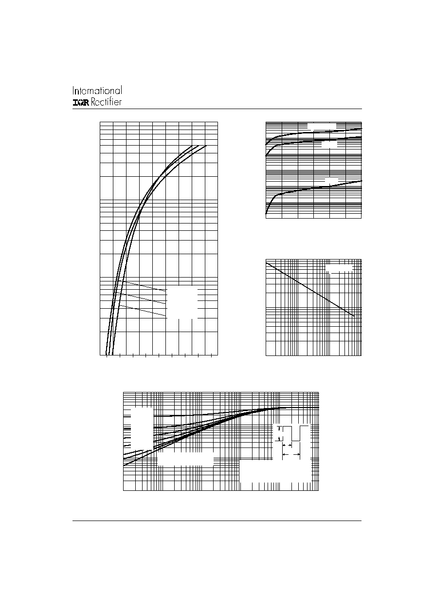
Fig. 2 - Typical Values Of Reverse Current
Vs. Reverse Voltage
Fig. 1 - Typical Forward Voltage Drop Characteristics
Reverse Voltage - V
R
(V)
Fig. 3 - Typical Junction Capacitance
Vs. Reverse Voltage
Forward Voltage Drop - V
FM
(V)
Instantaneous Forward Current - I
F
(A)
Reverse Current - I
R
(µA)
Reverse Voltage - V
R
(V)
Junction Capacitance - C
T
(pF)
Fig. 4 - Max. Thermal Impedance Z
thJC
Characteristics
t
1
, Rectangular Pulse Duration (Seconds)
Thermal Impedance Z
thJC
(°C/W)
1
10
100
1
10
100
1000
T = 25°C
J
0.1
1
10
00
0.4 0.8 1.2 1.6
2
2.4 2.8 3.2 3.6
4
T = 150°C
T = 125°C
T = 25°C
J
J
J
.01
0.1
1
10
0.00001
0.0001
0.001
0.01
0.1
1
Single Pulse
(Thermal Resistance)
D = 0.50
D = 0.20
D = 0.10
D = 0.05
D = 0.02
D = 0.01
2
t
1
t
P
DM
Notes:
1. Duty factor D = t1/ t2
2. Peak Tj = Pdm x ZthJC + Tc
0.001
0.01
0.1
1
10
100
1000
0
100
200
300
400
500
600
125°C
25°C
T = 150°C
J
HFA08SD60S
Bulletin PD-20618 rev. B 07/02
4
www.irf.com
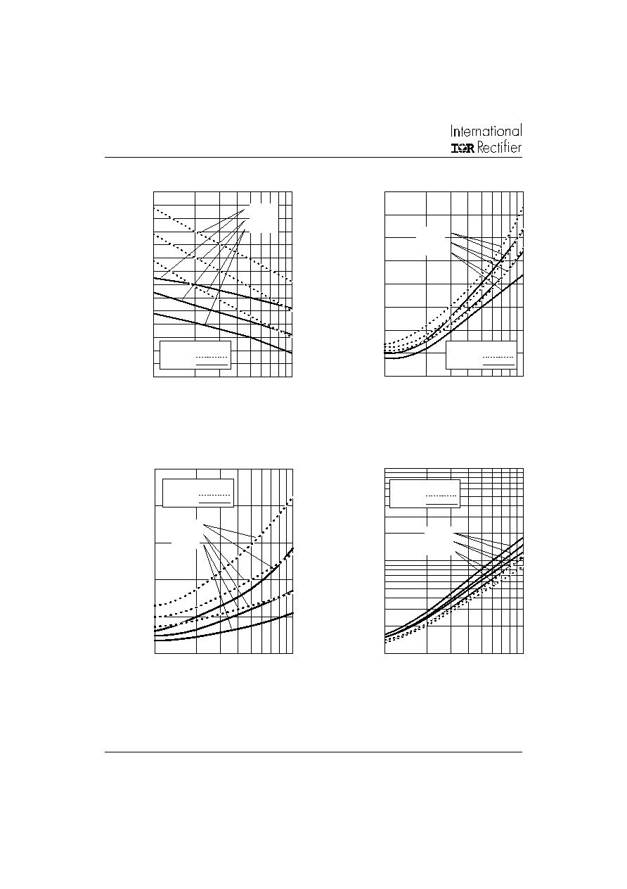
Fig. 5 - Typical Reverse Recovery vs. di
F
/dt
Fig. 6 - Typical Recovery Current vs. di
F
/dt
Irr (A)
Qrr ( nC )
di
(rec)M
/ dt (A/ µs)
di
F
/dt (A/ µs)
trr (ns)
Average Forward Current - I
F(AV)
(A)
Fig. 8 - Typical di
(rec)M
/dt vs. di
F
/dt
Fig. 7 - Typical Stored Charge vs. di
F
/dt
di
F
/dt (A/µs )
di
F
/dt (A/µs )
10
20
30
40
50
60
70
80
100
1000
If = 16A
If = 8A
If = 4A
Vr = 200V
Tj = 125°C
Tj = 25°C
100
1000
10000
100
1000
If = 16A
If = 8A
If = 4A
Vr = 200V
Tj = 125°C
Tj = 25°C
0
100
200
300
400
500
100
1000
If = 16A
If = 8A
If = 4A
Vr = 200V
Tj = 125°C
Tj = 25°C
0
5
10
15
20
100
1000
If = 16A
If = 8A
If = 4A
Vr = 200V
Tj = 125°C
Tj = 25°C
Bulletin PD-20618 rev. B 07/02
5
HFA08SD60S
www.irf.com
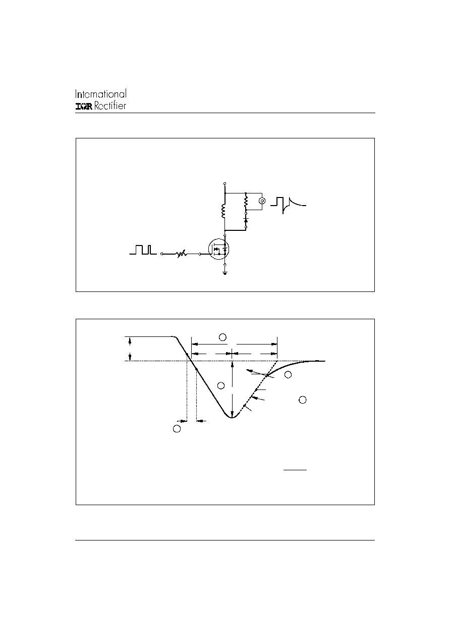
Fig. 10 - Reverse Recovery Waveform and Definitions
IRFP250
D.U.T.
L = 70µH
V = 200V
R
0.01
G
D
S
dif/dt
ADJUST
t
a
t
b
t
rr
Q
rr
I
F
I
RRM
I
RRM
0.5
di(rec)M/dt
0.75 I
RRM
5
4
3
2
0
1
di /dt
f
Fig. 9- Reverse Recovery Parameter Test Circuit
Reverse Recovery Circuit
di
F
/dt
di
F
/dt
4. Q
rr
- Area under curve defined by t
rr
and I
RRM
5. di(rec)M/dt - Peak rate of change of
current during tb portion of trr
1. di
F
/dt - Rate of change of current through zero
crossing
2. I
RRM
- Peak reverse recovery current
3. t
rr
- Reverse recovery time measured from zero
crossing point of negative going I
F
to point where
a line passing through 0.75 I
RRM
and 0.50 I
RRM
extrapolated to zero current
Q rr =
t rr x I RRM
2