Äîêóìåíòàöèÿ è îïèñàíèÿ www.docs.chipfind.ru
5/4/04
· Reduced RFI and EMI
· Reduced Snubbing
· Extensive Characterization of Recovery Parameters
· Hermetic
· Electrically Isolated
· Ceramic Eyelets
Features
Description
These Ultrafast, soft recovery diodes are optimized to reduce losses and EMI/RFI in high frequency power
conditioning systems. An extensive characterization of the recovery behavior for different values of current,
temperature and di/dt simplifies the calculations of losses in the operating conditions. The softness of the recovery
eliminates the need for a snubber in most applications. These devices are ideally suited for power converters, motors
drives and other applications where switching losses are significant portion of the total losses.
Ultrafast, Soft Recovery Diode
FRED
V
R
= 600V
V
F
= 1.9V
Q
rr
= 270nC
di
(rec)M
/dt = 345A/
µ
s
Note: D.C. = 50% rect. wave
1/2 sine wave, 60 Hz , P.W. = 8.33 ms
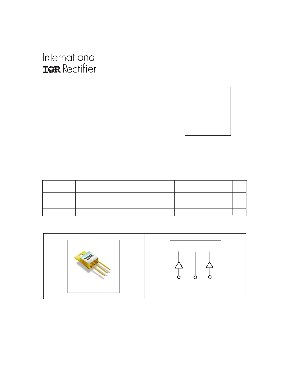
HFA35HB60C
www.irf.com
1
Parameter
Max.
Units
V
R
Cathode to Anode Voltage (Per Leg)
600
V
I
F(AV)
Continuous Forward Current,
T
C
=100 °C
30
I
FSM
Single Pulse Forward Current,
T
C
= 25°C (Per Leg)
150
P
D
@ T
C
= 25°C
Maximum Power Dissipation
63
W
T
J,
T
STG
Operating Junction and Storage Temperature Range
-55 to +150
°C
A
Absolute Maximum Ratings
CASE STYLE
TO-254AA
(ISOLATED BASE)
ANODE COMMON ANODE
CATHODE
PD - 20378B
2
www.irf.com
HFA35HB60C
See Fig. 2
Parameter
Min. Typ. Max. Units
Test Conditions
V
BR
Cathode Anode Breakdown Voltage 600
--
-- V I
R
= 250µA
Electrical Characteristics (Per Leg)@ T
J
= 25°C (unless otherwise specified)
L
S
Series Inductance
-- 6.7 -- nH
Measured from anode lead to cathode
lead , 6mm ( 0.025 in) from package
See Fig. 2
Thermal - Mechanical Characteristics
Parameter
Typ.
Max.
Units
R
thJC
Junction-to-Case, Single Leg Conducting
--
2.0
Wt
Weight
9.3
--
g
°C/W
V
F
Forward Voltage
--
--
1.9
I
F
= 15A
See Fig. 1
--
--
2.3
I
F
= 30A
-- -- 2.1
I
F
= 15A, T
J
= 125°C
V
I
R
Reverse Leakage Current --
--
10
µA
V
R
= V
R
Rated
C
T
Junction Capacitance, See Fig. 3 -- 24 36
-- -- 1.0 mA V
R
= 480V, T
J
= 125°C
pF V
R
= 200V
Dynamic Recovery Characteristics (Per Leg) @ T
J
= 25°C (unless otherwise specified)
A/µs
nC
A
Parameter
Min. Typ. Max. Units Test Conditions
t
rr1
Reverse Recovery Time
--
54
88
ns
T
J
= 25°C See Fig.
t
rr2
--
94
140
T
J
= 125°C 5
I
F
= 15A
I
RRM1
Peak Recovery Current
--
5.6
7.8
T
J
= 25°C See Fig.
I
RRM2
--
7.8 11.7
T
J
= 125°C 6
V
R
= 200V
Q
rr1
Reverse Recovery Charge
--
180
270
T
J
= 25°C See Fig.
Q
rr2
--
435
650
T
J
= 125°C 7
di
f
/dt = 200A/µs
di
(rec)M
/dt1
Peak Rate of Fall of Recovery Current
--
300
345
T
J
= 25°C See Fig.
di
(rec)M
/dt2
During t
b
--
190
285
T
J
= 125°C 8
www.irf.com
3
HFA35HB60C
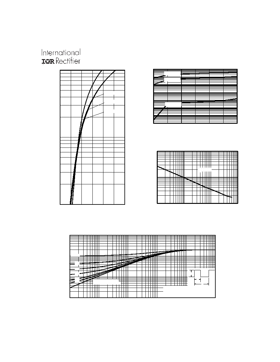
Fig. 4 - Maximum Thermal Impedance Z
thjc
Characteristics (Per Leg)
Fig. 2 - Typical Reverse Current Vs. Reverse
Voltage (Per Leg)
Fig. 3 - Typical Junction Capacitance Vs.
Reverse Voltage (Per Leg)
Fig. 1 - Maximum Forward Voltage Drop Vs.
Instantaneous Forward Current (Per Leg)
0.0001
0.001
0.01
0.1
1
10
100
1000
0
200
400
600
R
R
Reverse Voltage - V (V)
R
e
v
e
r
s
e
C
u
rr
e
n
t
- I
(µ
A
)
T = 25°C
J
T = 125°C
J
T = 150°C
J
10
100
1000
1
10
100
1000
T = 25°C
J
Reverse Voltage - V (V)
R
T
J
u
nction
C
a
p
a
cit
ance - C (p
F
)
A
0.01
0.1
1
10
0.00001
0.0001
0.001
0.01
0.1
1
Notes:
1. Duty factor D = t / t
2. Peak T = P
x Z
+ T
1
2
J
DM
thJC
C
P
t
t
DM
1
2
t , Rectangular Pulse Duration (sec)
T
her
m
a
l
Res
pons
e
(
Z
)
1
thJ
C
0.01
0.02
0.05
0.10
0.20
D = 0.50
SINGLE PULSE
(THERMAL RESPONSE)
0.0
1.0
2.0
3.0
4.0
5.0
6.0
Forward Voltage Drop -V F(V)
1
10
100
I
n
s
t
a
n
t
a
n
e
o
u
s
F
o
r
w
a
r
d
C
u
r
r
e
n
t
-
I
F
(
A
)
Tj = 125°C
Tj = 150°C
Tj = 25°C
4
www.irf.com
HFA35HB60C
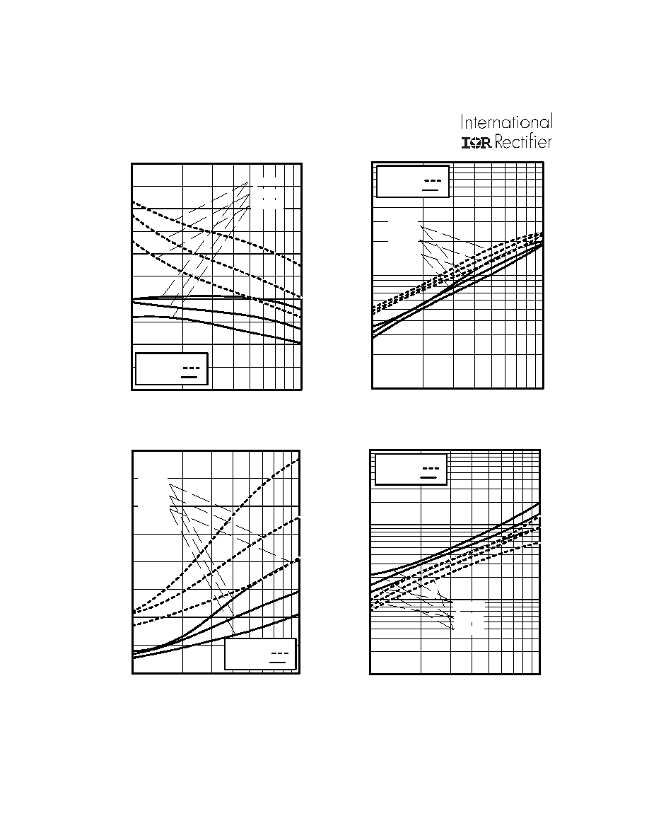
Fig. 7 - Typical Stored Charge Vs. di
f
/dt (Per Leg)
Fig. 8 - Typical di
(rec)M
/dt Vs. di
f
/dt (Per Leg)
Fig. 5 - Typical Reverse Recovery Vs. di
f
/dt (Per Leg)
Fig. 6 - Typical Recovery Current Vs. di
f
/dt (Per Leg)
0
30
60
90
120
150
100
1000
f
di /dt - (A/µs)
RR
Q
-
(n
C
)
I = 30A
I = 15A
I = 7.5A
F
F
F
V = 200V
T = 125°C
T = 25°C
R
J
J
1
10
100
100
1000
f
di /dt - (A/µs)
I
- (A
)
IRR
M
I = 30A
I = 15A
I = 7.5A
F
F
F
V = 200V
T = 125°C
T = 25°C
R
J
J
0
300
600
900
1200
100
1000
f
di /dt - (A/µs)
RR
Q
-
(nC
)
I = 30A
I = 15A
I = 7.5A
F
F
F
V = 200V
T = 125°C
T = 25°C
R
J
J
10
100
1000
10000
100
1000
f
di /dt - (A/µs)
d
i
(re
c
)
M
/
d
t
-
(A
/
µ
s
)
I = 15A
F
I = 7.5A
I = 30A
F
F
V = 200V
T = 125°C
T = 25°C
R
J
J
www.irf.com
5
HFA35HB60C
4. Q
rr
- Area under curve defined by t
rr
and I
RRM
t
rr
X I
RRM
Q
rr
=
2
5. di
(rec)M
/dt - Peak rate of change of
current during t
b
portion of t
rr
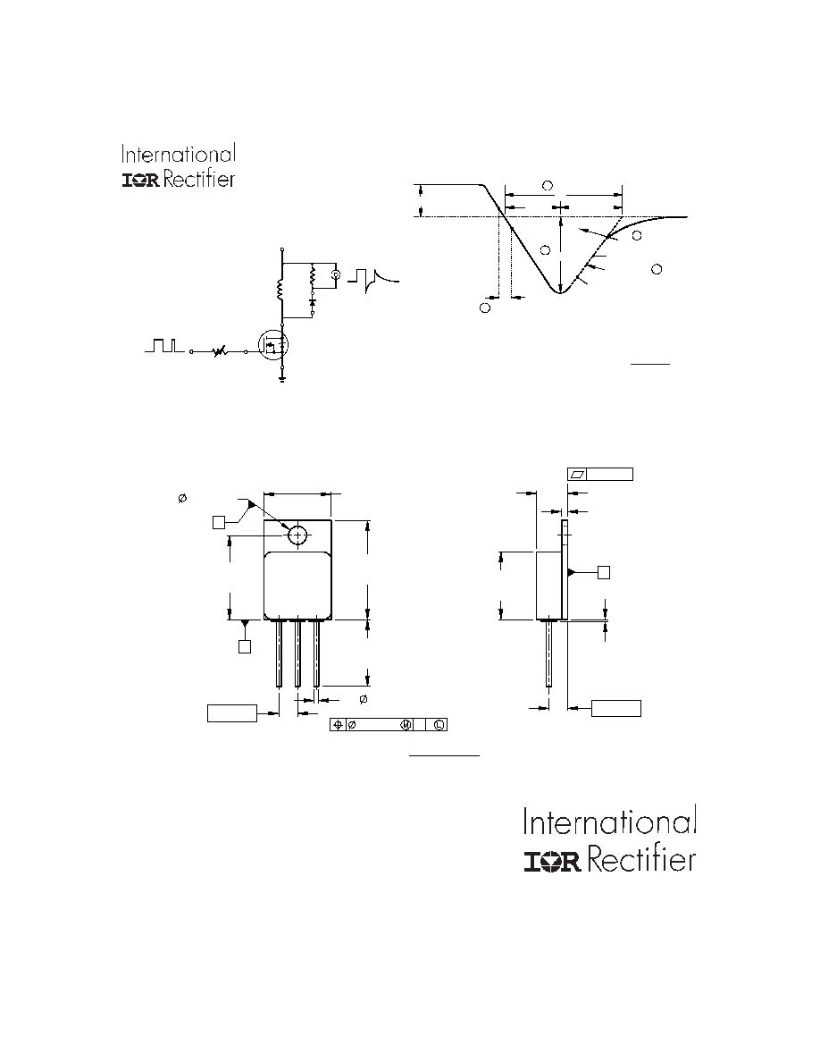
Fig. 10 - Reverse Recovery Waveform and Definitions
Fig. 9 - Reverse Recovery Parameter Test Circuit
t
a
t
b
t
rr
Q
rr
I
F
I
RRM
I
RRM
0.5
di(rec)M/dt
0.75 I
RRM
5
4
3
2
0
1
di /dt
f
1. di
f
/dt - Rate of change of current
through zero crossing
2. I
RRM
- Peak reverse recovery current
3. trr - Reverse recovery time measured
from zero crossing point of negative
going I
F
to point where a line passing
through 0.75 I
RRM
and 0.50 I
RRM
extrapolated to zero current
REVERSE RECOVERY CIRCUIT
IRFP250
D.U.T.
L = 70µH
V = 200V
R
0.01
G
D
S
dif/dt
ADJUST
Case Outline and Dimensions -- TO-254AA
6.60 [.260]
6.32 [.249]
1.27 [.050]
1.02 [.040]
0.12 [.005]
13.84 [.545]
13.59 [.535]
13.84 [.545]
13.59 [.535]
3.81 [.150]
2X
17.40 [.685]
16.89 [.665]
A
1.14 [.045]
0.89 [.035]
0.36 [.014]
B A
3X
B
20.32 [.800]
20.07 [.790]
3.78 [.149]
3.53 [.139]
1
2
3
17.40 [.685]
16.89 [.665]
3.81 [.150]
0.84 [.033]
MAX.
C
PIN ASSIGNMENTS
1 = ANODE 1
2 = COMMON CATHODE
3 = ANODE 2
NOT ES:
1. DIMENSIONING & TOLERANCING PER ASME Y14.5M-1994.
2. ALL DIMENS IONS ARE SHOWN IN MILLIMETERS [INCHES].
3. CONTROLLING DIMENSION: INCH.
4. CONFORMS TO JEDEC OUT LINE TO-254AA.
WORLD HEADQUARTERS: 233 Kansas St., El Segundo, California 90245, Tel: (310) 252-7105
IR LEOMINSTER: 205 Crawford St., Leominster, Massachusetts 01453, Tel: (978) 534-5776
Data and specifications subject to change without notice. 05/2004