 | ÐлекÑÑоннÑй компоненÑ: HFA90NH40 | СкаÑаÑÑ:  PDF PDF  ZIP ZIP |
90nh40
PD -2.468 rev. B 02/99
Reduced RFI and EMI
Reduced Snubbing
Extensive Characterization of
Recovery Parameters
Features
Description
HEXFRED
T M
diodes are optimized to reduce losses and EMI/RFI in high frequency
power conditioning systems. An extensive characterization of the recovery
behavior for different values of current, temperature and di/dt simplifies the
calculations of losses in the operating conditions. The softness of the recovery
eliminates the need for a snubber in most applications. These devices are
ideally suited for power converters, motors drives and other applications where
switching losses are significant portion of the total losses.
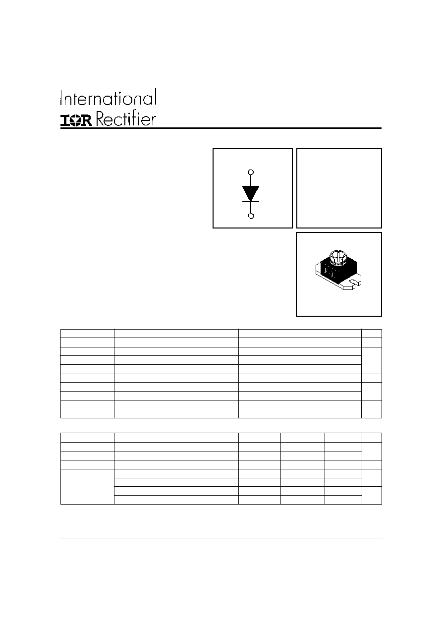
Ultrafast, Soft Recovery Diode
HEXFRED
TM
HFA90NH40
LUG
TERMINAL
ANODE
BASE CATHODE
d
a
HALF-PAK
V
R
= 400V
V
F
(typ.)
= 1V
I
F(AV)
= 90A
Q
rr
(typ.) = 420nC
I
RRM
(typ.)
= 9.3A
t
rr
(typ.)
= 36ns
di
(rec)M
/dt (typ.)
= 260A/µs
Thermal - Mechanical Characteristics
Absolute Maximum Ratings (per Leg)
lbfin
(Nm)
°C/W
K/W
Parameter
Min.
Typ.
Max.
Units
R
thJC
Junction-to-Case
0.40
R
thCS
Case-to-Sink, Flat, Greased Surface
0.15
Wt
Weight
26 (0.9)
g (oz)
Mounting Torque
15 (1.7)
25 (2.8)
Terminal Torque
30 (3.4)
40 (4.6)
Vertical Pull
35
2 inch Lever Pull
35
Parameter
Max.
Units
V
R
Cathode-to-Anode Voltage
400
V
I
F
@ T
C
= 25°C
Continuous Forward Current
170
I
F
@ T
C
= 100°C
Continuous Forward Current
84
I
FSM
Single Pulse Forward Current
600
E
AS
Non-Repetitive Avalanche Energy
1.4
mJ
P
D
@ T
C
= 25°C
Maximum Power Dissipation
310
P
D
@ T
C
= 100°C
Maximum Power Dissipation
125
T
J
Operating Junction and
T
STG
Storage Temperature Range
-55 to +150
W
A
°C
lbfin
Note: Limited by junction temperature
Mounting surface must be smooth, flat, free or burrs or other
L = 100µH, duty cycle limited by max T
J
protrusions. Apply a thin even film or thermal grease to mounting
125°C
surface. Gradually tighten each mounting bolt in 5-10 lbfin steps
until desired or maximum torque limits are reached. Module
1
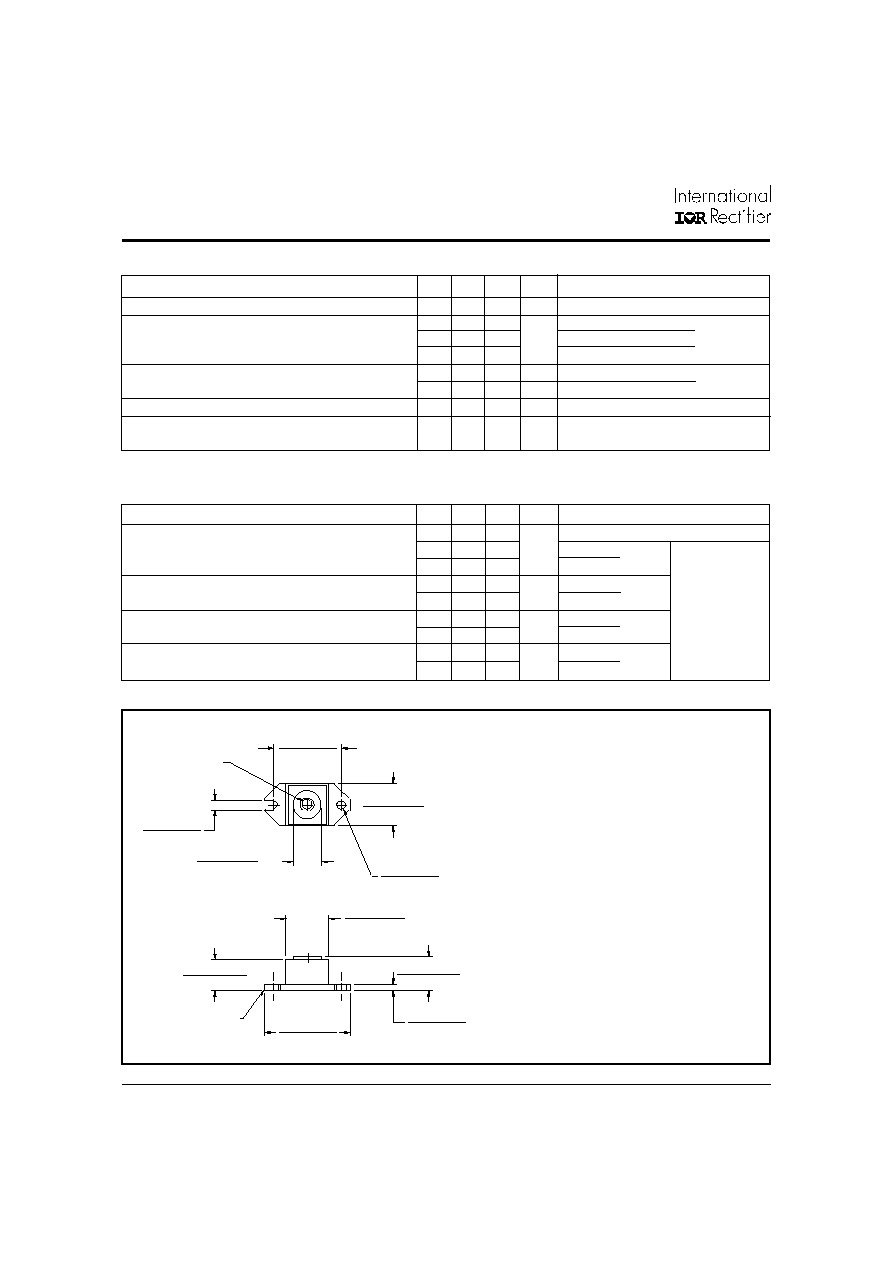
HFA90NH40
PD-2.468 rev. B 02/99
2
30.40 (1.197)
29.90 (1.177)
18.42 (0.725)
19.69 (0.775)
12.83 (0.505)
12.57 (0.495)
DIA.
4.11 (0.162)
3.86 (0.152)
19.18 (0.755)
18.92 (0.745)
SQ.
13.59 (0.535)
14.10 (0.555)
15.75 (0.620)
14.99 (0.590)
3.05 (0.120)
3.30 (0.130)
38.61 (1.520)
39.62 (1.560)
DIA.
3.86 (0.152)
4.11 (0.162)
1/4-20 UNC-2B
Dimensions in millimeters and inche
1
2
LEAD ASSIGNMENTS
1 - ANODE
2 - CATHODE
H P
ALF- AK
Parameter
Min. Typ. Max. Units
Test Conditions
V
BR
Cathode Anode Breakdown Voltage
400
V
I
R
= 100µA
V
FM
Max Forward Voltage
1.1
1.3
I
F
= 90A
1.3
1.5
V
I
F
= 180A
1.0
1.2
I
F
= 90A, T
J
= 125°C
I
RM
Max Reverse Leakage Current
1.0
6.0
µA
V
R
= V
R
Rated
1.5
8.0
mA
T
J
= 125°C, V
R
= 320V
C
T
Junction Capacitance
180 260
pF
V
R
= 200V
From top of terminal hole to mounting
plane
Electrical Characteristics (per Leg) @ T
J
= 25°C (unless otherwise specified)
Dynamic Recovery Characteristics (per Leg) @ T
J
= 25°C (unless otherwise specified)
A/µs
nC
A
L
S
Series Inductance
7.0
nH
Parameter
Min. Typ. Max. Units Test Conditions
t
rr
Reverse Recovery Time
36
I
F
= 1.0A, di
f
/dt = 200A/µs, V
R
= 30V
t
rr1
See Fig. 5
90
140
ns T
J
= 25°C
t
rr2
160 240
T
J
= 125°C
I
F
= 90A
I
RRM1
Peak Recovery Current
9.3
17
T
J
= 25°C
I
RRM2
See Fig. 6
15
30
T
J
= 125°C
V
R
= 200V
Q
rr1
Reverse Recovery Charge
420 1100
T
J
= 25°C
Q
rr2
See Fig. 7
1200 3200
T
J
= 125°C
di
f
/dt = 200A/µs
di
(rec)M
/dt1
Peak Rate of Fall of Recovery Current
360
T
J
= 25°C
di
(rec)M
/dt2
During t
b
See Fig. 8
260
T
J
= 125°C
See Fig. 1
See Fig. 2
See Fig. 3
HFA90NH40
PD-2.468 rev. B 02/99
3
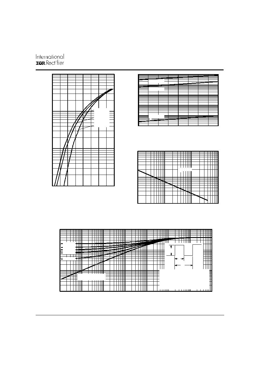
Fig. 4 - Maximum Thermal Impedance Z
thJC
Characteristics
Fig. 2 - Typical Reverse Current vs. Reverse
Voltage
Fig. 3 - Typical Junction Capacitance vs.
Reverse Voltage
Fig. 1 - Maximum Forward Voltage Drop
vs. Instantaneous Forward Current
1
10
100
1000
0.4
0.8
1.2
1.6
2.0
FM
F
Ins
tant
aneo
us F
orward
Curre
nt - I
(A)
Forward Voltage Drop - V (V)
T = 150°C
T = 125°C
T = 25°C
J
J
J
0.1
1
10
100
1000
10000
0
100
200
300
400
R
R
Reverse Voltage - V (V)
T = 150°C
Reverse Cu
rrent -
I (
µA)
T = 125°C
T = 25°C
J
J
J
100
1000
10000
1
10
100
1000
T = 25°C
J
Reverse Voltage - V (V)
R
T
Ju
nction
Capacit
ance - C
(pF)
A
0.001
0.01
0.1
1
0.00001
0.0001
0.001
0.01
0.1
1
10
100
1
th
JC
t , Rectangular Pulse Duration (Seconds)
D = 0.50
D = 0.33
D = 0.25
D = 0.17
D = 0.08
Single Pulse
(Thermal Resistance)
T
h
er
m
a
l
I
m
pe
danc
e -
Z
(
K
/
W
)
2
t
1
t
P
DM
Notes:
1. Duty factor D = t / t
2. Peak T = P x Z + T
J
DM
thJC
C
2
1
HFA90NH40
PD-2.468 rev. B 02/99
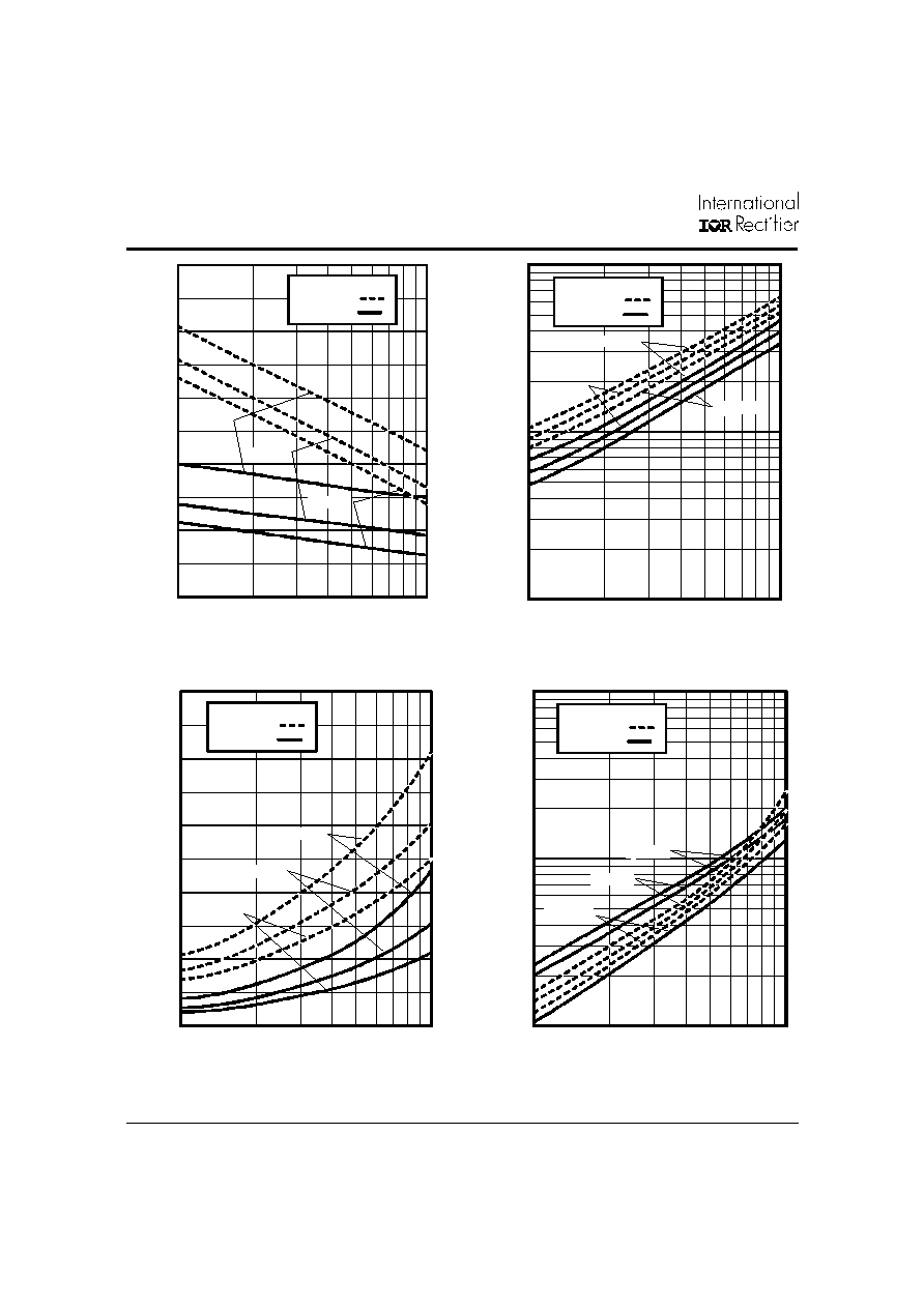
4
Fig. 7 - Typical Stored Charge vs. di
f
/dt
Fig. 8 - Typical di
(rec)M
/dt vs. di
f
/dt
Fig. 5 - Typical Reverse Recovery vs. di
f
/dt
Fig. 6 - Typical Recovery Current vs. di
f
/dt
40
80
120
160
200
240
100
1000
f
di /dt - (A/µs)
t
- (ns
)
rr
I = 200A
I = 40A
I = 90A
F
F
F
V = 200V
T = 125°C
T = 25°C
R
J
J
0
1000
2000
3000
4000
5000
100
1000
f
di /dt - (A/µs)
RR
Q
- (nC)
I = 40A
I = 200A
I = 90A
V = 200V
T = 125°C
T = 25°C
R
J
J
F
F
F
100
1000
10000
100
1000
f
di /dt - (A/µs)
di(rec)M/dt
- (A/
µs)
I = 200A
I = 40A
I = 90A
V = 200V
T = 125°C
T = 25°C
R
J
J
F
F
F
1
10
100
100
1000
f
di /dt - (A/µs)
I
- (A)
I
RRM
I = 200A
I = 40A
I = 90A
F
F
F
V = 200V
T = 125°C
T = 25°C
R
J
J
HFA90NH40
PD-2.468 rev. B 02/99
5
4. Q
rr
- Area under curve defined by t
rr
and I
RRM
t
rr
X I
RRM
Q
rr
=
2
5. di
(rec)M
/dt - Peak rate of change of
current during t
b
portion of t
rr
V
(AVAL)
R(RATED)
I
L(PK)
V
DECAY
TIME
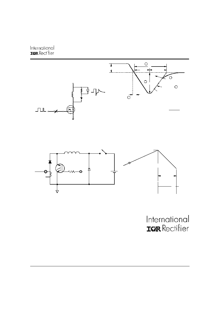
Fig. 11 - Avalanche Test Circuit and Waveforms
Fig. 10 - Reverse Recovery Waveform and
Definitions
Fig. 9 - Reverse Recovery Parameter Test
Circuit
t
a
t
b
t
rr
Q
rr
I
F
I
RRM
I
RRM
0.5
di(rec)M/dt
0.75 I
RRM
5
4
3
2
0
1
di /dt
f
1. di
f
/dt - Rate of change of current
through zero crossing
2. I
RRM
- Peak reverse recovery current
3. trr - Reverse recovery time measured
from zero crossing point of negative
going I
F
to point where a line passing
through 0.75 I
RRM
and 0.50 I
RRM
extrapolated to zero current
REVERSE RECOVERY CIRCUIT
IRFP250
D.U.T.
L = 70µH
V = 200V
R
0.01
G
D
S
dif/dt
ADJUST
CURRENT
MONITOR
HIGH-SPEED
SWITCH
DUT
Rg = 25 ohm
+
FREE-WHEEL
DIODE
Vd = 50V
L = 100µH
http://www.irf.com Fax-On-Demand: +44 1883 733420 Data and specifications subject to change without notice.
233 Kansas St., El Segundo, California 90245 U.S.A. Tel: (310) 322 3331. Fax: (310) 322 3332.
Hurst Green, Oxted, Surrey RH8 9BB, U.K. Tel: ++ 44 1883 732020. Fax: ++ 44 1883 733408.
15 Lincoln Court, Brampton, Markham, Ontario L6T3Z2. Tel: (905) 453 2200. Fax: (905) 475 8801.
Saalburgstrasse 157, 61350 Bad Homburg. Tel: ++ 49 6172 96590. Fax: ++ 49 6172 965933.
Via Liguria 49, 10071 Borgaro, Torino. Tel: ++ 39 11 4510111. Fax: ++ 39 11 4510220.
K&H Bldg., 2F, 30-4 Nishi-Ikebukuro 3-Chome, Toshima-Ku, Tokyo, Japan 171. Tel: 81 3 3983 0086.
1 Kim Seng Promenade, Great World City West Tower,13-11, Singapore 237994. Tel: ++ 65 838 4630.
16 Fl. Suite D.207, Sec. 2, Tun Haw South Road, Taipei, 10673, Taiwan. Tel: 886 2 2377 9936.
WORLD HEADQUARTERS:
EUROPEAN HEADQUARTERS:
IR CANADA:
IR GERMANY:
IR ITALY:
IR FAR EAST:
IR SOUTHEAST ASIA:
IR TAIWAN: