FULLY PROTECTED LOW SIDE SWITCH
Data Sheet No. PD60235
IPS1011(
S
)(
R
)
INTELLIGENT POWER LOW SIDE SWITCH
Features
·
Over temperature shutdown
·
Over current shutdown
·
Active clamp
e
·
Low current & logic lev l input
On/Off for EMI
) is a three terminal Intelligent Power
·
ESD protection
·
Optimized Turn
·
Diagnostic on the input current
Description
The IPS1011(S)(R
Switch (IPS) that features a low side MOSFET with over-
current, over-temperature, ESD protection and drain to
source active clamp. This device offers protections and
the high reliability required in harsh environments. The
switch provides efficient protection by turning OFF the
power MOSFET when the temperature exceeds 165°C or
when the drain current reaches 85A. The device restarts
once the input is cycled. A serial resistance connected to
the input provides the diagnostic.
The avalanche capability
is significantly enhanced by the active clamp and covers
most inductive load demagnetizations.
Product Summary
Rds(on) 13m
(
max.)
Vclamp 36V
Ishutdown 85A (typ.)
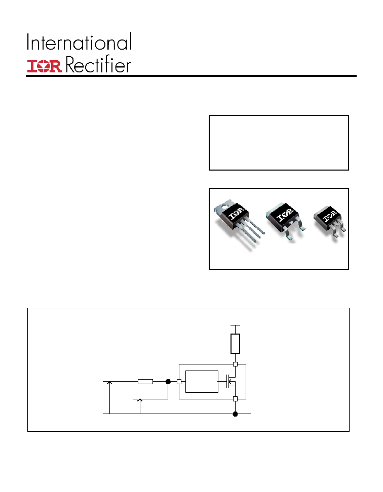
Packages
TO-220 D²Pak D-Pak
IPS1011 IPS1011S IPS1011R
Typical Connection
S
Control
IN
Input R
D
Load
+Bat
Input Signal
V Diag
1
2
3
www.irf.com
1
IPS1011(
S
)(
R
)
Absolute Maximum Ratings
Absolute maximum ratings indicate sustained limits beyond which damage to the device may occur. All voltage parameters
are referenced to Ground lead. (Tambient=25°C unless otherwise specified).
Symbol Parameter
Min.
Max.
Units
Vds
Maximum drain to source voltage
-0.3
36
V
Vds cont.
Maximum continuous drain to source voltage
-
28
V
Vin
Maximum input voltage
-0.3
6
V
Isd cont.
Max diode continuous current (limited by thermal dissipation)
5 A
Maximum power dissipation (internally limited by thermal protection)
Rth=5°C/W
IPS1011
25
Rth=40°C/W
IPS1011S
1" sqr. footprint
3.1
Pd
Rth=50°C/W
IPS1011R
1" sqr. footprint
2.5
W
Electrostatic discharge voltage (Human body) C=100pF, R=1500
Between drain and source
4
Other combinations
3
Electrostatic discharge voltage (Machine Model) C=200pF,R=0
Between drain and source
0.5
ESD
Other combinations
0.3
kV
Tj max.
Max. storage & operating temperature junction temperature
-40
150
°C
Tsoldering
Lead soldering temperature (10 seconds)
300 °C
Thermal Characteristics
Symbol Parameter
Typ.
Max.
Units
Rth1
Thermal resistance junction to ambient IPS1011
TO-220 free air
50
Rth2
Thermal resistance junction to case IPS1011 TO-220
1.2
Rth1
Thermal resistance junction to ambient IPS1011S
D²Pak std. footprint
60
Rth2
Thermal resistance junction to ambient IPS1011S D²Pak 1" sqr. footprint
40
Rth3
Thermal resistance junction to case IPS1011S
D²Pak 1.2
Rth1
Thermal resistance junction to ambient IPS1011R
D-Pak std. footprint
70
Rth2
Thermal resistance junction to ambient IPS1011R
D-Pak 1" sqr. footprint
50
Rth3
Thermal resistance junction to case IPS1011R
D-Pak 1.2
°C/W
Recommended Operating Conditions
These values are given for a quick design. For operation outside these conditions, please consult the application notes.
Symbol Parameter
Min.
Max.
Units
VIH
High level input voltage
4.5
5.5
VIL
Low level input voltage
0
0.5
Continuous drain current, Tambient=85°C, Tj=125°C, Vin=5V
Rth=5°C/W
IPS1011
18
Rth=40°C/W
IPS1011S
1" sqr. Footprint
6.5
Ids
Rth=50°C/W
IPS1011R
1" sqr. Footprint
6
A
Rin
Recommended resistor in series with IN pin to generate a diagnostic
0.5
10
k
Max L
Max recommended load inductance (including line inductance) (1)
5 µH
Max F
Max frequency (switching losses = conduction losses)
200 Hz
Max t rise
Max Input rising time
1 µs
(1) Higher inductance is possible if maximum load current is limited - see figure 11
www.irf.com
2
IPS1011(
S
)(
R
)
Static Electrical Characteristics
Tj=25°C, Vcc=14V (unless otherwise specified)
Symbol Parameter
Min.
Typ.
Max.
Units
Test
Conditions
ON state resistance Tj=25°C
10 13
Rds(on)
ON state resistance Tj=150°C (2)
19 25
m
Vin=5V, Ids=30A
Idss1
Drain to source leakage current
0.1 10
Vcc=14V,
Tj=25°C
Idss2
Drain to source leakage current
0.2 20
µA
Vcc=28V, Tj=25°C
V clamp1
Drain to source clamp voltage 1
36
39
Id=20mA
V clamp2
Drain to source clamp voltage 2
40 42
Id=5A
Vin clamp
IN to source pin clamp voltage
5.5
6.5
7.5
Iin=1mA
Vth
Input threshold voltage
1.7
V
Id=10mA
Switching Electrical Characteristics
Vcc=14V, Resistive load=0.5
, Rinput=50
, Vin=5V, Tj=25°C
Symbol Parameter
Min.
Typ.
Max.
Units
Test
Conditions
Tdon
Turn-on delay time to 20%
15
50
150
Tr
Rise time 20% to 80%
20
50
100
Tdoff
Turn-off delay time to 80%
100
330
1000
Tf
Fall time 80% to 20%
30
70
150
µs
See figure 2
Eon + Eoff
Turn on and off energy
5
mJ
Protection Characteristics
Symbol Parameter
Min.
Typ.
Max.
Units
Test
Conditions
Tsd
Over temperature threshold
150(2)
165
°C
See figure 1
Isd
Over current threshold
60
85
110
A
See figure 1
OV
Over voltage protection (not active when
the device is ON )
34 37
V
Vreset
IN protection reset threshold
1.7
V
Treset
Time to reset protection 15(2)
50
200
µs
Vin=0V
Diagnostic
Symbol Parameter
Min.
Typ.
Max.
Units
Test
Conditions
Iin, on
ON state IN positive current
15
32
70
Iin, off
OFF state IN positive current
(after protection latched )
150 230 350 µA
Vin=5V
Vin=5V
(2) Guaranteed by design
www.irf.com
3
IPS1011(
S
)(
R
)
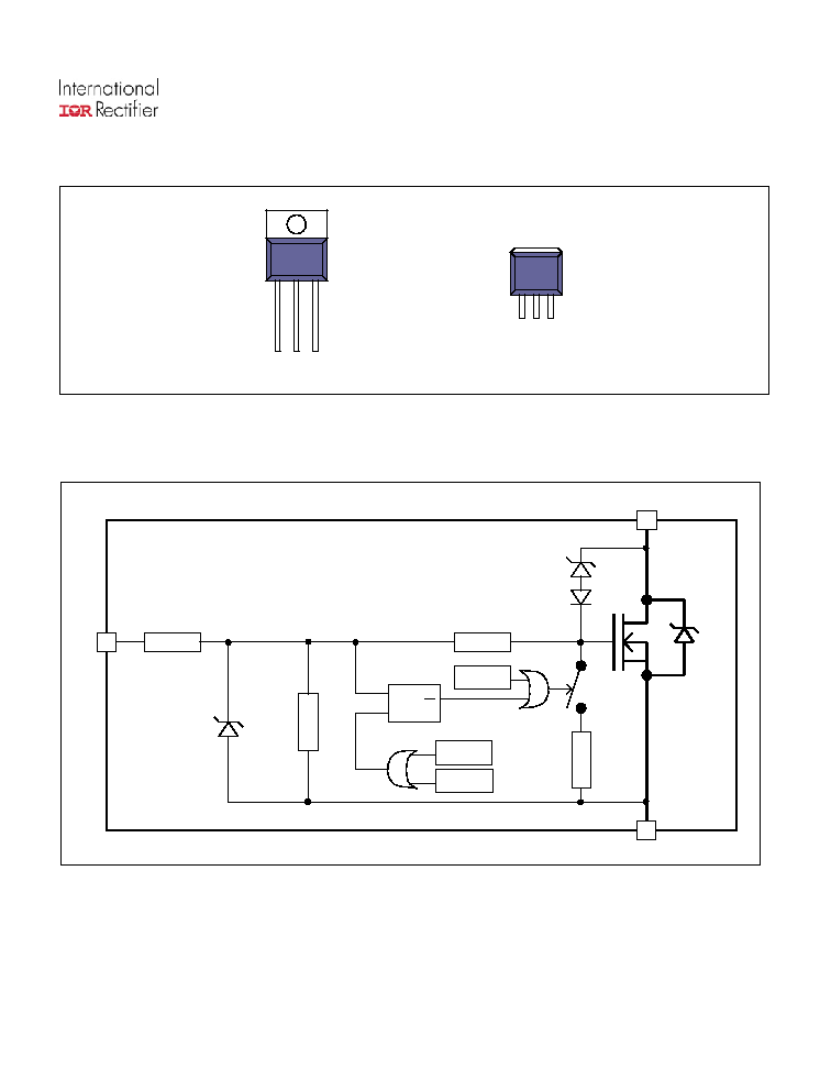
Lead Assignments
1 2 3
TO220
1- In
2- D
3- S
2 - Drain
1 2 3
D²Pak D Pak
2 - Drain
Functional Block Diagram
All values are typical
IN
S
R
Q
6.5V
Tj > 165°C
DRAIN
SOURCE
37V
15k
I > Isd
75
43V
Vds > O.V.
2k
150k
www.irf.com
4
IPS1011(
S
)(
R
)
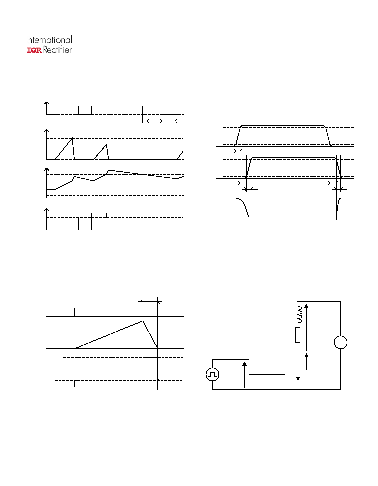
All curves are typical values. Operating in the shaded area is not recommended.
Tj
Isd
Tsd
165°C
Ids
Vin
Ishutdown
Tshutdown
t<T reset
t>T reset
Vdiag
fault
normal
Vds
Ids
Vin
Tr-in
80%
20%
80%
20%
Td on
Tr
Td off
Tf
Figure 1 Timing diagram
Figure 2 IN rise time & switching definitions
Vds
Ids
Vin
IN
D
S
R
L
0V
5V
14V
+
-
V load
Rem : During active clamp,
Vload is negative
Vds
Ids
Vin
Vcc
Vds clamp
T clamp
See Application Notes to evaluate power dissipation
Figure 3 Active clamp waveforms
Figure 4 Active clamp test circuit
www.irf.com
5
Document Outline