 | ÐлекÑÑоннÑй компоненÑ: IR01HD214 | СкаÑаÑÑ:  PDF PDF  ZIP ZIP |
Äîêóìåíòàöèÿ è îïèñàíèÿ www.docs.chipfind.ru
Data Sheet No. PD-6.075-G
IR01H(D)214 / IR01H(D)214-P2
IR01H(D)224 / IR01H(D)224-P2
IR01H(D)420 / IR01H(D)420-P2
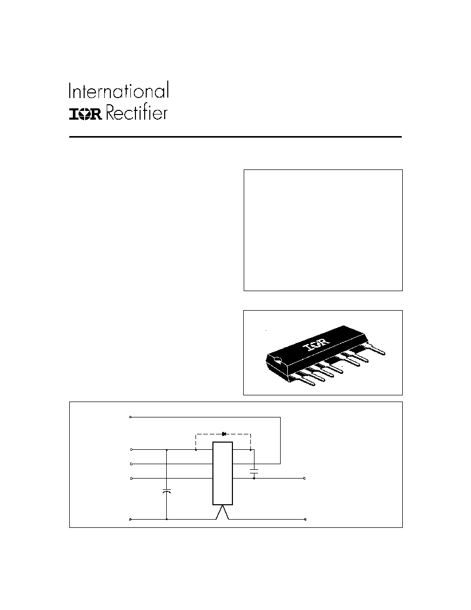
Typical Connection
Features
·
Output Power MOSFETs in half-bridge configuration
·
500V rated breakdown voltage
·
High side gate drive designed for bootstrap
operation
·
Matched propagation delay for both channels
·
Undervoltage lockout
·
5V Schmitt-triggered input logic
·
Half-Bridge output in phase with HIN
·
Heatsink version (P2) with improved PD
Description
The IR01H(D)xxx is a high voltage, high speed half
bridge. Proprietary HVIC and latch immune CMOS
technologies, along with the HEXFET power
MOSFET technology, enable ruggedized single
package construction. The logic inputs are compat-
ible with standard CMOS or LSTTL outputs. The
front end features an independent high and low side
driver in phase with the logic compatible input
signals. The output features two HEXFETs in a half-
bridge configuration with a high pulse current buffer
stage designed for minimum cross-conduction in the
half bridge. Propagation delays for the high and low
side power MOSFETs are matched to simplify use.
HIGH VOLTAGE HALF BRIDGE
1
Packages
Product Summary
250V- 214/224
500V - 420
t
on/off
130 & 90 ns
t
rr
260 ns
R
DS
(on)
2.0
- H214
1.1
- H224
3.0
- H420
P
D
(T
A
= 25
o
C)
2.0W
4.0W - P2
V
IN (max)
HV DC Bus
NOTE: D1 is not required for
the HD type
V I N
C O M
H
IN
1
2
3
4
6
7
9
Vcc
C O M
V O
V
IN
V
B
T O
L O A D
H
IN
L
IN
V c c
L
IN
D1
2
IR01H(D)214 / IR01H(D)214-P2
IR01H(D)224 / IR01H(D)224-P2
IR01H(D)420 / IR01H(D)420-P2
Absolute Maximum Ratings
Absolute Maximum Ratings indicate sustained limits beyond which damage to the device may occur. All voltage param-
eters are absolute voltages referenced to COM, all currents are defined positive into any lead. The Thermal Resistance
and Power Dissipation ratings are measured under board mounted and still air conditions.
Symbol
Definition
Min.
Max.
Units
V
IN
High Voltage Supply
214/224
-0.3
250
420
-0.3
500
V
B
High Side Floating Supply Absolute Voltage
214/224
-0.3
275
420
-0.3
525
VO
Half-Bridge Output
-0.3
V
IN
+ 0.3
V
V
IH
/V
IL
Logic Input Voltage (HIN & LIN)
- 0.3
V
cc
+ 0.3
V
V
CC
Low Side and Logic Fixed Supply Voltage
-0.3
25
V
dV/dt
Peak Diode Recovery dv/dt
--
3.50
V/ns
P
D
Package Power Dissipation @ T
A
+25
o
C
--
2
W
- P2
4.0
W
R
THJA
Thermal Resistance, Junction to Ambient
--
60
°C/W
- P2
30
o
C/W
R
THJC
Thermal Resistance, Junction to Case (heatsink)
- P2
--
20
°C/W
T
J
Junction Temperature
-55
150
°C
T
S
Storage Temperature
-55
150
o
C
T
L
Lead Temperature (Soldering, 10 seconds)
--
300
°C
W
V
3
IR01H(D)214 / IR01H(D)214-P2
IR01H(D)224 / IR01H(D)224-P2
IR01H(D)420 / IR01H(D)420-P2
Recommended Operating Conditions
The Input/Output logic timing diagram is shown in Figure 1. For proper operation the device should be used within the
recommended conditions.
Symbol
Definition
Min.
Max.
Units
V
B
High Side Floating Supply Absolute Voltage
V
O
+ 10
V
O
+ 20
V
V
IN
High Voltage Supply
214/224
--
250
V
420
--
500
V
O
Half-Bridge Output Voltage
214/224
(note 1)
250
V
420
--
500
V
CC
Low Side and Logic Fixed Supply Voltage
10
20
V
V
IH
/V
IL
Logic Input Voltage (HIN & LIN)
0
V
CC
V
T
A
Ambient Temperature
-40
125
o
C
Id
Continuous Drain Current (TA = 25
o
C)
214
--
0.85
A
214-P2
--
1.4
224
--
1.1
224-P2
--
1.9
420
--
0.7
420-P2
--
1.1
(TA = 85
o
C)
214
--
0.55
A
214-P2
--
0.9
224
--
0.7
224-P2
--
1.4
420
--
0.5
420-P2
--
0.8
(TC = 25
o
C)
214-P2
--
1.7
224-P2
--
2.3
420-P2
--
1.4
Note 1:
Logic operational for VO of -5 to 250V (214/224) and 500V (420).
Logic state held for V0 of -5 to -V
B
A
V
4
IR01H(D)214 / IR01H(D)214-P2
IR01H(D)224 / IR01H(D)224-P2
IR01H(D)420 / IR01H(D)420-P2
Dynamic Electrical Characteristics
V
BIAS
(V
CC
, V
BS
) = 15V and T
A
= 25°C unless otherwise specified. Switching time waveform definitions are shown in
figure 2.
Symbol
Definition
Min.
Typ. Max. Units Test Conditions
t
on
Turn-On Propagation Delay (see note 2)
--
130
200
Vs = 0V
t
off
Turn-Off Propagation Delay (see note 2)
--
90
200
Vs = 500V
t
r
Turn-On Rise Time (see note 2)
--
80
120
ns
t
f
Turn-Off Fall Time (see note 2)
--
40
70
MT
Delay Matching, HS & LS Turn-On/Off
--
30
--
t
rr
Reverse Recovery Time (MOSFET Body Diode)
--
260
--
I
F
= 0.7A
Qrr
Reverse Recovery Charge (MOSFET Body Diode)
--
0.7
--
µC
di/dt
= 100 A/us
Note 2: Switching times as specified and illustrated in figure 2 are referenced to the MOSFET gate input
voltage. This is shown as HO in figure 2.
Static Electrical Characteristics
V
BIAS
(V
CC
, V
B
) = 15V and T
A
= 25°C unless otherwise specified. The Input voltage and current levels are referenced to
COM.
Symbol
Definition
Min.
Typ. Max. Units Test Conditions
V
CCUV+
V
CC
Supply Undervoltage Positive Going
8.8
9.3
9.8
V
Threshold
V
CCUV-
V
CC
Supply Undervoltage Negative Going
7.5
8.2
8.6
V
Threshold
I
QCC
Quiescent V
CC
Supply Current
--
140
240
µA
I
QBS
Quiescent V
BS
Supply Current
--
20
50
µA
I
os
Offset Supply Leakage Current
--
--
50
µA
V
B
= V
S
= 500V
V
IH
Logic "1" Input Voltage
2.7
--
--
V
V
CC
= 10V to 20V
V
IL
Logic "0" Input Voltage
--
--
0.8
V
V
CC
= 10V to 20V
I
IN+
Logic "1" Input Bias Current
--
20
40
I
IN-
Logic "0" Input Bias Current
--
--
1.0
Rds(on)
Static Drain-to-Source On-Resistance
214
--
2.0
--
Id=850mA/T
J
=150
o
C
224
--
1.1
--
Id=1.1A/T
J
=150
o
C
420
--
3.0
--
Id=700mA/T
J
=150
o
C
V
SD
Diode Forward Voltage
214/420
--
0.8
--
V
Id=700mA/T
J
=150
o
C
224
--
0.85
--
Id=1.1A/T
J
=150
o
C
V
V V
CC
= 10V to 20V
µA
5
IR01H(D)214 / IR01H(D)214-P2
IR01H(D)224 / IR01H(D)224-P2
IR01H(D)420 / IR01H(D)420-P2
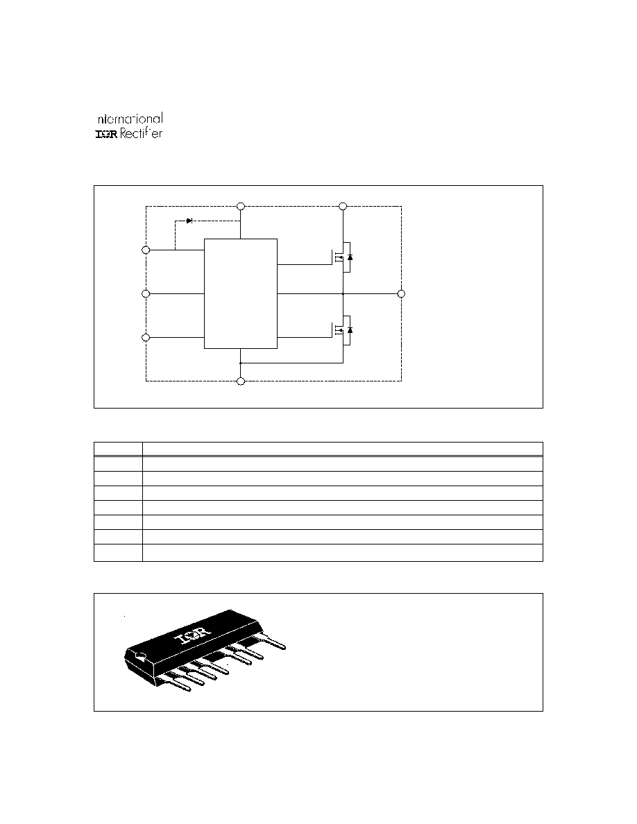
Functional Block Diagram
Lead Assignments
Lead Definitions
Symbol
Description
VCC
Logic and internal gate drive supply voltage.
HIN
Logic input for high side Half Bridge output, in phase
LIN
Logic input for low side Half Bridge output, in phase
V
B
High side gate drive floating supply
V
+
High voltage supply
VO
Half Bridge output
COM
Logic and low side of Half Bridge return
1
Vcc
2
HIN
3
LIN
4
COM
6 VB
7 VO
9 VIN
9
7
6
4
3
2
1
NOTE: xxx = 214 or 224 or 420
D1 included in HD type only
I R 2 1 0 1
VIN
V
B
C O M
V O
V c c
H
IN
L
IN
1
2
3
4
6
7
9
H
O
V
S
L
O
IRFCxxx
IRFCxxx
NOTE: xxx = 214 or 224 or 420
D 1