 | –≠–ª–µ–∫—Ç—Ä–æ–Ω–Ω—ã–π –∫–æ–º–ø–æ–Ω–µ–Ω—Ç: IRFM260 | –°–∫–∞—á–∞—Ç—å:  PDF PDF  ZIP ZIP |
Product Summary
Part Number
BV
DSS
R
DS(on)
I
D
IRFM260
200V
0.060
35A*
Features:
n
Hermetically Sealed
n
Electrically Isolated
n
Simple Drive Requirements
n
Ease of Paralleling
n
Ceramic Eyelet
Absolute Maximum Ratings
Parameter
IRFM260
Units
ID @ VGS = 10V, TC = 25∞C
Continuous Drain Current
35*
ID @ VGS = 10V, TC = 100∞C Continuous Drain Current
28
IDM
Pulsed Drain Current
180
PD @ TC = 25∞C
Max. Power Dissipation
250
W
Linear Derating Factor
2.0
W/K
VGS
Gate-to-Source Voltage
±20
V
EAS
Single Pulse Avalanche Energy
700
mJ
IAR
Avalanche Current
35
A
EAR
Repetitive Avalanche Energy
25
mJ
dv/dt
Peak Diode Recovery dv/dt
4.3
V/ns
TJ
Operating Junction
-55 to 150
TSTG
Storage Temperature Range
Lead Temperature
300(0.063 in.(1.6mm) from case for 10s)
Weight
9.3 (typical)
g
N-CHANNEL
Provisional Data Sheet No. PD-9.1388A
Pre-Radiation
200Volt, 0.060
, HEXFET
HEXFET technology is the key to International
Rectifier's advanced line of power MOSFET tran-
sistors. The efficient geometry design achieves very
low on-state resistance combined with high
transconductance.
HEXFET transistors also feature all of the well-es-
tablished advantages of MOSFETs, such as volt-
age control, very fast switching, ease of paralleling
and electrical parameter temperature stability. They
are well-suited for applications such as switching
power supplies, motor controls, inverters, choppers,
audio amplifiers and high-energy pulse circuits, and
virtually any application where high reliability is re-
quired.
HEXFET transistor's totally isolated package elimi-
nates the need for additional isolating material be-
tween the device and the heatsink. This improves
thermal efficiency and reduces drain capacitance.
o
C
A
REPETITIVE AVALANCHE AND dv/dt RATED
IRFM260
HEXFET
Æ
TRANSISTOR
Next Data Sheet
Index
Previous Datasheet
To Order
IRFM260
Electrical Characteristics
@ Tj = 25∞C (Unless Otherwise Specified)
Parameter
Min
Typ
Max Units
Test Conditions
BVDSS
Drain-to-Source Breakdown Voltage
200
--
--
V
VGS =0 V, ID = 1.0mA
BVDSS/
TJ Temperature Coefficient of Breakdown
--
0.24
--
V/∞C
Reference to 25∞C, ID = 1.0mA
Voltage
RDS(on)
Static Drain-to-Source
--
--
0.060
VGS = 10V, ID = 28A
On-State Resistance
--
--
0.068
VGS = 10V, ID = 35A
VGS(th)
Gate Threshold Voltage
2.0
--
4.0
V
VDS = VGS, ID = 250µA
gfs
Forward Transconductance
22
--
--
S (
)
VDS > 15V, IDS = 28A
IDSS
Zero Gate Voltage Drain Current
--
--
25
VDS= 0.8 x Max Rating,VGS=0V
--
--
250
VDS = 0.8 x Max Rating
VGS = 0V, TJ = 125∞C
IGSS
Gate-to-Source Leakage Forward
--
--
100
VGS = 20 V
IGSS
Gate-to-Source Leakage Reverse
--
--
-100
VGS = -20V
Qg
Total Gate Charge
--
--
230
VGS = 10V, ID = 35A
Qgs
Gate-to-Source Charge
--
--
40
nC
VDS = Max Rating x 0.5
Qgd
Gate-to-Drain (`Miller') Charge
--
--
110
td
(on)
Turn-On Delay Time
--
--
29
VDD = 100V, ID = 35A,
tr
Rise Time
--
--
120
RG = 2.35
td
(off)
Turn-Off Delay Time
--
--
110
tf
Fall Time
--
--
92
LD
Internal Drain Inductance
--
8.7
--
LS
Internal Source Inductance
--
8.7
--
Ciss
Input Capacitance
--
5100
--
VGS = 0V, VDS = 25 V
Coss
Output Capacitance
--
1100
--
pF
f = 1.0MHz
Crss
Reverse Transfer Capacitance
--
280
--
Source-Drain Diode Ratings and Characteristics
Parameter
Min Typ Max Units
Test Conditions
IS
Continuous Source Current (Body Diode)
--
--
35*
ISM
Pulse Source Current (Body Diode)
--
--
180
VSD
Diode Forward Voltage
--
--
1.8
V
T
j
= 25∞C, IS = 35A, VGS = 0V
trr
Reverse Recovery Time
--
--
420
ns
Tj = 25∞C, IF = 35A, di/dt
100A/
µ
s
QRR
Reverse Recovery Charge
--
--
4.9
µ
C
VDD
50V
ton
Forward Turn-On Time
Intrinsic turn-on time is negligible. Turn-on speed is substantially controlled by LS + LD.
A
Modified MOSFET symbol
showing the integral reverse
p-n junction rectifier.
Thermal Resistance
Parameter
Min Typ Max
Units
Test Conditions
RthJC
Junction-to-Case
--
--
0.50
RthCS
Case-to-Sink
--
0.21
--
K/W
Mounting surface flat, smooth, and greased
RthJA
Junction-to-Ambient
--
--
48
Typical socket mount
nA
nH
ns
Measured from drain lead,
6mm (0.25 in) from package
to center of die.
Measured from source lead,
6mm (0.25 in) from package
to source bonding pad.
Modified MOSFET symbol show-
ing the internal inductances.
µ
A
Next Data Sheet
Index
Previous Datasheet
To Order

IRFM260
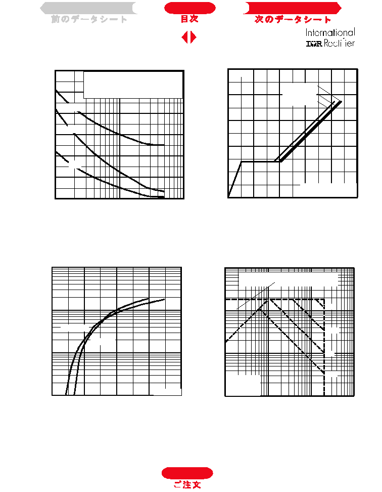
Fig 4. Normalized On-Resistance
Vs. Temperature
Fig 2. Typical Output Characteristics,
T
J
= 150
o
C
Fig 1. Typical Output Characteristics,
T
J
= 25
o
C
Fig 3. Typical Transfer Characteristics
0 . 0
0 . 5
1 . 0
1 . 5
2 . 0
2 . 5
- 6 0
- 4 0
- 2 0
0
2 0
4 0
6 0
8 0
1 0 0
1 2 0
1 4 0
1 6 0
J
T , Ju nctio n T emp eratu re (∞C)
R
,
D
r
a
i
n
-
to
-
S
o
u
r
c
e
O
n
R
e
s
i
s
t
a
n
c
e
D
S
(
on)
(
N
o
r
m
a
l
i
z
ed)
V = 10 V
G S
A
I = 46 A
D
1
1 0
1 0 0
1 0 0 0
0 . 1
1
1 0
1 0 0
I
,
D
r
a
i
n-
t
o
-
S
ou
r
c
e
C
u
r
r
ent
(
A
)
D
V , D ra in-to-S ou rce V o lta ge (V )
D S
VGS
TOP 15V
10V
8.0V
7.0V
6.0V
5.5V
5.0V
BOTT OM 4.5V
2 0µ s PU LSE W ID TH
T = 2 5∞C
C
A
4.5 V
1
1 0
1 0 0
1 0 0 0
0 . 1
1
1 0
1 0 0
I
,
D
r
a
i
n
-
t
o
-
S
our
c
e
C
u
r
r
ent
(
A
)
D
V , Dra in -to-So urce V oltag e (V)
D S
VGS
TOP 15V
10V
8.0V
7.0V
6.0V
5.5V
5.0V
BOTT OM 4.5V
20µ s PU L SE W ID TH
T = 1 50 ∞C
A
4.5 V
J
1
1 0
1 0 0
1 0 0 0
4
5
6
7
8
9
1 0
T = 2 5 ∞C
T = 1 5 0 ∞C
J
J
G S
V , Ga te -to -S o u rce V o lta g e (V )
D
I
, D
r
a
i
n
-
to
-
S
o
u
r
c
e
C
u
r
r
e
n
t
(
A
)
V = 5 0 V
2 0 µ s PU L SE W ID TH
D S
A
To Order
Next Data Sheet
Index
Previous Datasheet
IRFM260
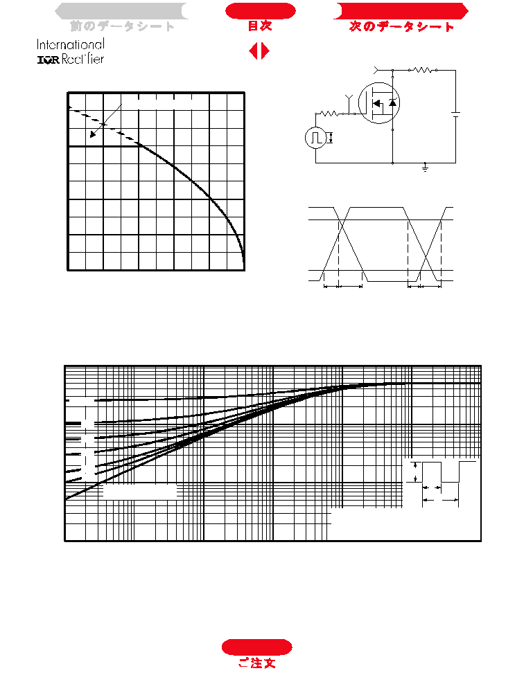
Fig 8. Maximum Safe Operating Area
Fig 6. Typical Gate Charge Vs.
Gate-to-Source Voltage
Fig 5. Typical Capacitance Vs.
Drain-to-Source Voltage
Fig 7. Typical Source-Drain Diode
Forward Voltage
0
2 0 0 0
4 0 0 0
6 0 0 0
8 0 0 0
1 0 0 0 0
1 2 0 0 0
1
1 0
1 0 0
C
,
C
a
pac
i
t
anc
e (
p
F
)
D S
V , Dra in-to-So urce V olta ge (V )
A
V = 0 V , f = 1 M H z
C = C + C , C S H O R T E D
C = C
C = C + C
G S
iss gs gd ds
rss gd
oss d s gd
C
is s
C
o s s
C
rs s
0
4
8
1 2
1 6
2 0
0
5 0
1 0 0
1 5 0
2 0 0
2 5 0
Q , T ota l G ate Ch arge (n C)
G
V
,
G
a
te
-
t
o
-
S
o
u
r
c
e
V
o
l
t
a
g
e
(
V
)
GS
A
FO R TEST C IRC U IT
SEE FIG UR E 13
I = 35 A
V = 16 0V
V = 10 0V
V = 40 V
D
DS
DS
DS
1
1 0
1 0 0
1 0 0 0
1
1 0
1 0 0
1 0 0 0
V , Dra in -to-So urce Vo ltag e (V)
D S
I ,
D
r
a
i
n
C
u
r
r
e
n
t
(
A
)
OPE R ATIO N IN TH IS A RE A LI MI TE D
BY R
D
D S(o n)
T = 25 ∞C
T = 15 0∞C
S ing le Pulse
C
J
10µ s
100µ s
1m s
10 ms
A
1
1 0
1 0 0
1 0 0 0
0 . 0
1 . 0
2 . 0
3 . 0
4 . 0
T = 2 5∞C
T = 15 0∞C
J
J
V = 0 V
G S
V , S o urce-to -Drain Vo lta ge (V )
I
, R
e
v
e
r
s
e
D
r
a
i
n
C
u
r
r
e
n
t
(
A
)
S D
SD
A
To Order
Next Data Sheet
Index
Previous Datasheet
IRFM260
Fig 11. Maximum Effective Transient Thermal Impedance, Junction-to-Case
Fig 9. Maximum Drain Current Vs.
Case Temperature
0 . 0 0 1
0 . 0 1
0 . 1
1
0 . 0 0 0 0 1
0 . 0 0 0 1
0 . 0 0 1
0 . 0 1
0 . 1
1
1 0
t , Re cta n g u lar P ul se D u ra tio n (se c )
1
th
J
C
D = 0.50
0.01
0.02
0.05
0.10
0.20
SING LE P ULSE
(T HERMA L RES PO NSE)
A
T
her
m
al R
e
s
pon
s
e
(
Z
)
P
t 2
1
t
D M
N otes :
1 . D uty fac tor D = t / t
2. P eak T = P x Z + T
1
2
J
D M
th J C
C
Fig 10a. Switching Time Test Circuit
V
DS
90%
10%
V
GS
t
d(on)
t
r
t
d(off)
t
f
Fig 10b. Switching Time Waveforms
V
DS
Pulse Width
1
µs
Duty Factor
0.1 %
R
D
V
GS
R
G
D.U.T.
10V
+
-
V
DD
0
1 0
2 0
3 0
4 0
5 0
2 5
5 0
7 5
1 0 0
1 2 5
1 5 0
C
I
,
D
r
ai
n
C
u
r
r
ent
(
A
m
p
s
)
D
T , C ase T emp era ture (∞C)
A
LIM ITE D B Y P ACK AG E
To Order
Next Data Sheet
Index
Previous Datasheet