Äîêóìåíòàöèÿ è îïèñàíèÿ www.docs.chipfind.ru
Absolute Maximum Ratings
Parameter
Units
ID @ VGS = -10V, TC = 25°C
Continuous Drain Current
-6.5
ID @ VGS = -10V, TC = 100°C Continuous Drain Current
-4.1
I D M
Pulsed Drain Current
-25
PD @ TC = 25°C
Max. Power Dissipation
25
W
Linear Derating Factor
0.20
W/°C
VGS
Gate-to-Source Voltage
±20
V
EAS
Single Pulse Avalanche Energy
92
mJ
IAR
Avalanche Current
--
A
EAR
Repetitive Avalanche Energy
--
mJ
dv/dt
Peak Diode Recovery dv/dt
-5.5
V/ns
TJ
Operating Junction
-55 to 150
TSTG
Storage Temperature Range
Lead Temperature
300 (0.063 in. (1.6mm) from case for 10s)
Weight
0.98(typical)
g
PD - 90550D
The HEXFET
technology is the key to International
Rectifier's advanced line of power MOSFET transistors.
The efficient geometry and unique processing of this latest
"State of the Art" design achieves: very low on-state resis-
tance combined with high transconductance.
The HEXFET transistors also feature all of the well
established advantages of MOSFETs such as volt-
age control, very fast switching, ease of parelleling
and temperature stability of the electrical parameters.
They are well suited for applications such as switch-
ing power supplies, motor controls, inverters, chop-
pers, audio amplifiers and high energy pulse circuits.
o
C
A
04/20/01
www.irf.com
1
TO-39
Product Summary
Part Number BVDSS R
DS(on)
I
D
IRFF9130 -100V 0.30
-6.5A
Features:
n
Repetitive Avalanche Ratings
n
Dynamic dv/dt Rating
n
Hermetically Sealed
n
Simple Drive Requirements
n
Ease of Paralleling
For footnotes refer to the last page
JANTX2N6849
REPETITIVE AVALANCHE AND dv/dt RATED
JANTXV2N6849
H E X F E T
T R A N S I S T O R S
JANS2N6849
THRU-HOLE (TO-205AF)
REF:MIL-PRF-19500/564
100V, P-CHANNEL
IRFF9130
IRFF9130
2
www.irf.com
Thermal Resistance
Parameter
Min Typ Max
Units
Test Conditions
RthJC
Junction-to-Case
--
--
5.0
RthJA
Junction-to-Ambient
--
--
175 Typical socket mount
°C/W
Source-Drain Diode Ratings and Characteristics
Parameter
Min Typ Max Units
Test Conditions
IS
Continuous Source Current (Body Diode)
--
--
-6.5
ISM
Pulse Source Current (Body Diode)
--
--
-25
VSD
Diode Forward Voltage
--
--
-4.7
V
T
j
= 25°C, IS =-6.5A, VGS = 0V
trr
Reverse Recovery Time
--
--
250
nS
Tj = 25°C, IF = -6.5A, di/dt
-100A/
µ
s
QRR
Reverse Recovery Charge
--
--
3.0
µC
VDD
-50V
ton
Forward Turn-On Time
Intrinsic turn-on time is negligible. Turn-on speed is substantially controlled by LS + LD.
A
Note: Corresponding Spice and Saber models are available on the G&S Website.
For footnotes refer to the last page
Electrical Characteristics
@ Tj = 25°C (Unless Otherwise Specified)
Parameter
Min
Typ Max Units
Test Conditions
BVDSS
Drain-to-Source Breakdown Voltage
-100
--
--
V
VGS = 0V, ID = -1.0mA
BVDSS/
TJ
Temperature Coefficient of Breakdown
--
-0.10
--
V/°C
Reference to 25°C, ID = -1.0mA
Voltage
RDS(on)
Static Drain-to-Source On-State
--
-- 0.30 VGS = -10V, ID = -4.1A
Resistance
--
-- 0.345
VGS =-10V, ID =-6.5A
VGS(th)
Gate Threshold Voltage
-2.0
--
-4.0 V VDS = VGS, ID = -250
µ
A
gfs
Forward Transconductance
2.5
--
--
S (
)
VDS > -15V, IDS = -4.1A
IDSS
Zero Gate Voltage Drain Current
--
--
-25
VDS= -80V, VGS=0V
--
--
-250
µA
VDS = -80V
VGS = 0V, TJ = 125°C
IGSS
Gate-to-Source Leakage Forward
--
--
-100
VGS = -20V
IGSS
Gate-to-Source Leakage Reverse
--
--
100
nA
VGS = 20V
Qg
Total Gate Charge
14.7
--
34.8
VGS =-10V, ID = -6.5A
Qgs
Gate-to-Source Charge
1.0
--
7.1
nC
VDS= -50V
Qgd
Gate-to-Drain (`Miller') Charge
2.0
--
21
td
(on)
Turn-On Delay Time
--
--
60
VDD = -50V, ID = -6.5A,
tr
Rise Time
--
--
140
VGS =-10V,RG =7.5
td
(off)
Turn-Off Delay Time
--
--
140
tf
Fall Time
--
--
140
LS + LD
Total Inductance
--
7.0
--
Ciss
Input Capacitance
--
800
VGS = 0V, VDS = -25V
Coss
Output Capacitance
--
350
--
pF
f = 1.0MHz
Crss
Reverse Transfer Capacitance
--
125
--
nH
ns
Measured from drain lead (6mm/0.25in. from
package) to source lead (6mm/0.25in. from
package)
www.irf.com
3
IRFF9130
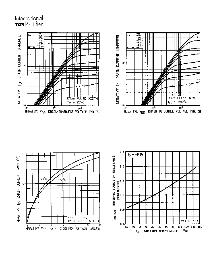
Fig 4. Normalized On-Resistance
Vs. Temperature
Fig 2. Typical Output Characteristics
Fig 1. Typical Output Characteristics
Fig 3. Typical Transfer Characteristics
IRFF9130
4
www.irf.com
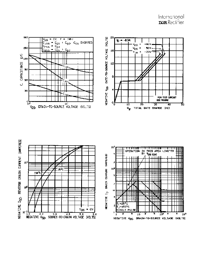
Fig 8. Maximum Safe Operating Area
Fig 6. Typical Gate Charge Vs.
Gate-to-Source Voltage
Fig 5. Typical Capacitance Vs.
Drain-to-Source Voltage
Fig 7. Typical Source-Drain Diode
Forward Voltage
13 a& b
13 a& b
www.irf.com
5
IRFF9130
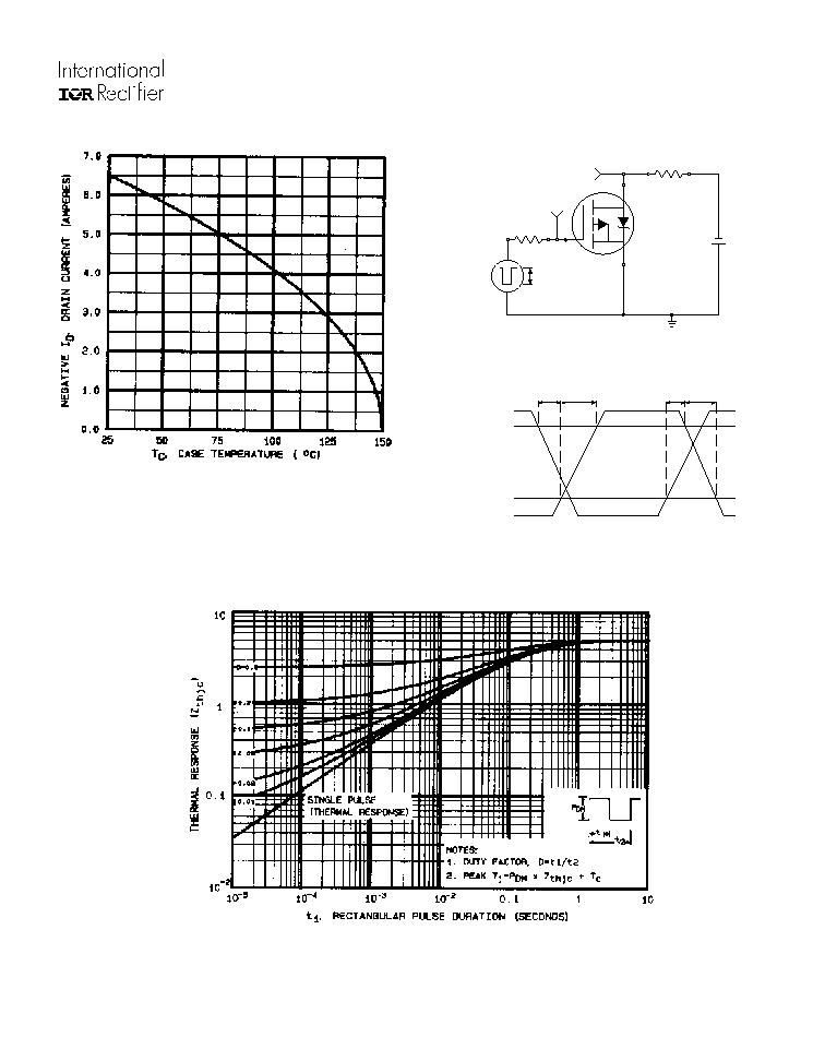
Fig 11. Maximum Effective Transient Thermal Impedance, Junction-to-Case
Fig 9. Maximum Drain Current Vs.
Case Temperature
Fig 10a. Switching Time Test Circuit
Fig 10b. Switching Time Waveforms
V
DS
V
GS
Pulse Width
1
µs
Duty Factor
0.1 %
R
D
V
GS
V
DD
R
G
D.U.T.
+
-
V
DS
90%
10%
V
GS
t
d(on)
t
r
t
d(off)
t
f