 | –≠–ª–µ–∫—Ç—Ä–æ–Ω–Ω—ã–π –∫–æ–º–ø–æ–Ω–µ–Ω—Ç: OM186SM | –°–∫–∞—á–∞—Ç—å:  PDF PDF  ZIP ZIP |

3.5 - 43
3.5
Three Terminal, Adjustable Low Dropout
2.0 Amp And 1.0 Amp Positive
Voltage Regulators
4 11 R0
SURFACE MOUNT LOW DROPOUT POSITIVE
ADJUSTABLE REGULATOR
FEATURES
∑ Hermetic Surface Mount Package
∑ Operates Down To 1V Dropout, 1.5V @ Max. Current
∑ .020% Line Regulation Typically
∑ .050% Load Regulation Typically
∑ 1% Reference Voltage
∑ Electrically Equivalent To LT1085 And LT1086
∑ Available Hi-Rel Screened
DESCRIPTION
These three terminal positive adjustable voltage regulators in a surface mount
package are designed to provide 2.0 Amps and 1.0 Amp with higher efficiency than
conventional voltage regulators. The devices are designed to operate to 1 Volt input
to output differential and the dropout voltage is specified as a function of load current.
These devices are ideally suited for Hi-Rel applications where surface mount, small
size, hermeticity and high reliability are required.
ABSOLUTE MAXIMUM RATINGS
@ 25∞C
Input Voltage . . . . . . . . . . . . . . . . . . . . . . . . . . . . . . . . . . . . . . . . . . . . . . . . . . . . . . . . . . . 35 V
Operating Junction Temperature Range . . . . . . . . . . . . . . . . . . . . . . . . - 55∞C to + 150∞C
Storage Temperature Range . . . . . . . . . . . . . . . . . . . . . . . . . . . . . . . . . . - 55∞C to + 150∞C
Output Current - OM185SM. . . . . . . . . . . . . . . . . . . . . . . . . . . . . . . . . . . . . . . . . . 2.0 A
Output Current -
OM186SM. . . . . . . . . . . . . . . . . . . . . . . . . . . . . . . . . . . . . . . . . . 1.0 A
Thermal Resistance - OM185SM . . . . . . . . . . . . . . . . . . . . . . . . . . . . . . . . . . . . . . . . 9∞C/W
Thermal Resistance -
OM186SM . . . . . . . . . . . . . . . . . . . . . . . . . . . . . . . . . . . . . . . 14∞C/W
Lead Temperature (Soldering 10 Seconds) . . . . . . . . . . . . . . . . . . . . . . . . . . . . . . . . 280∞C
OM185SM/SR/NR
OM186SM/SR/NR
3.5 - 44
OM185SM/SR/NR - OM186SM/SR/NR
3.5
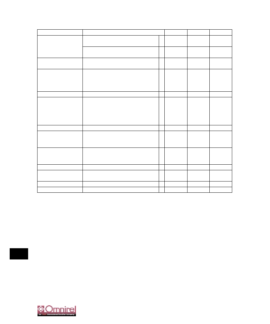
ELECTRICAL CHARACTERISTICS
(T
J
= -55∞C to +125∞C)
Parameter
Conditions
Min.
Max.
Units
Reference Voltage
I
OUT
= 10mA, T
j
= 25∞C
(V
IN
- V
OUT
) = 3V1.238
1.262
V
10mA I
OUT
I
FULL LOAD
1.5V (V
IN
- V
OUT
) 25 V (Note 3)
∑
1.220
1.270
V
Line Regulation
I
LOAD
= 10mA, 1.5V (V
IN
-V
OUT
) 15V, T
j
= 25∞C
0.25
%
15V (V
IN
- V
OUT
) 35V (Notes 1 & 2)
∑
0.6
%
Load Regulation
(V
IN
- V
OUT
) = 3V
10mA I
OUT
I
FULL LOAD
T
j
= 25∞C (Notes 1, 2, & 3)
1.0
%
∑
1.2
%
Dropout Voltage
V
REF
= 1%, I
OUT
= I
FULL LOAD
∑
1.5
V
Current Limit
OM185SM
(V
IN
- V
OUT
) = 5V
∑
2.0
A
(V
IN
- V
OUT
) = 25V
∑
0.10
A
OM186SM
(V
IN
- V
OUT
) = 5V
∑
1.0
A
(V
IN
- V
OUT
) = 25V
∑
0.05
A
Minimum Load Current
(V
IN
- V
OUT
) = 25V
∑
15
mA
Thermal Regulation
T
A
= 25∞C, 30 ms pulse
OM185SM
0.025
%/W
OM186SM
0.055
%/W
Ripple Rejection
f = 120Hz
C
ADJ
= 25µF Tantalum
I
OUT
- I
FULL LOAD
(V
IN
- V
OUT
) = 3V60
dB
Adjust Pin Current
T
J
= 25∞C
120
µA
Adjust Pin Current Change
10mA I
OUT
I
FULL LOAD
1.5V (V
IN
- V
OUT
) 25V
∑
5
µA
Temperature Stability
-55∞C T
J
+150∞C
1
%
Long Term Stability
T
A
= 125∞C, 1000 Hrs.
1
%
Note 1: Load and line regulation are measured at a constant junction temperature by low duty cycle pulse testing.
Note 2: Line and load regulation are guaranteed up to the maximum power dissipation (OM185/20W, OM186/10W).
Power dissipation is determined by the input/output differential and the output current. Guaranteed maximum
power dissipation will not be available over the full input/output voltage range.
Note 3: I
FULL LOAD
curve is defined as the minimum value of current limit as a function of input to output voltage. Note that
power dissipation is only achievable over a limited range of input to output voltage.
Note 4: Dropout voltage is specified over the full output current range of the device.
The
∑
denotes the specifications which apply over the full operating temperature range.
3.5 - 45
OM185SM/SR/NR - OM186SM/SR/NR
3.5
TYPICAL PERFORMANCE CHARACTERISTICS
OM185SM
TEMPERATURE STABILITY
REFERENCE VOLTAGE (V)
1.230
-50
TEMPERATURE (∞C)
150
1.270
1.240
1.250
1.260
-25
0
25
50
75 100 125
OM185SM
LOAD REGULATION
OUTPUT VOLTAGE DEVIATION (%)
-0.20
-50
TEMPERATURE (∞C)
150
0.10
-0.15
-0.10
-0.05
0
0.05
-25
0
25
50
75 100 125
OM186SM
TEMPERATURE STABILITY
TEMPERATURE (∞C)
150
OUTPUT VOLTAGE CHANGE (%)
-50 -25
0
50
75
125
-2.0
0
1.0
2.0
-1.0
25
100
OM186SM
LOAD REGULATION
TEMPERATURE (∞C)
150
-50
-25
25 50
75
125
-0.20
-0.15
-0.10
0
0.05
0.10
I= 1A
-0.05
0
100
OUTPUT VOLTAGE DEVIATION (%)
I= 2A
OM185SM
SHORT CIRCUIT CURRENT
SHORT CIRCUIT CURRENT (A)
0
0
INPUT/OUTPUT DIFFERENTIAL (V)
5
10
15
20
25
30
35
1
2
3
4
5
-55∞C
25∞C
150∞C
FULL LOAD
I
OM186SM
SHORT CIRCUIT CURRENT
INPUT/OUTPUT DIFFERENTIAL (V)
T
j
= -55∞C
SHORT CIRCUIT CURRENT (A)
0
5
10
15
20
25
30
0
0.5
1
1.5
2
T
j
= 25∞C
GUARANTEED
OUTPUT CURRENT
T
j
= 150∞C

OM185SM/SR/NR - OM186SM/SR/NR
3.5
MECHANICAL OUTLINES
.450
SQ.
.300
4 PLCS.
.050
24 PLCS.
.305
SQ.
.02 x 45∞
.090
MAX.
.05 X 45∞
MAX. 3 PLCS.
.009 R.
28 PLCS.
.035
PIN 1
PIN 28
BOTTOM
TOP
SIDE
4
1
26
12
18
Pin Connection
Pin 1, 15 thru 28:
IN
Pin 2, 3, 13, and 14:
ADJ
Pin 4 thru 12:
OUT
D2
1. ADJ
2. Vout
3. Vin
1
2
3
.450
.140
.415
.157
.015
.140
.140
.050
.050
.037
.375
.030
MIN.
TOP VIEW
SIDE VIEW
BOTTOM VIEW
.625
SMD-1
LCC-28