3.1 - 147
3.1
500 Volt, 5 And 10 Amp, N-Channel IGBT
With a Soft Recovery Diode
In A Hermetic Metal Package
4 11 R2
Supersedes 2 07 R1
INSULATED GATE BIPOLAR TRANSISTOR
(IGBT) IN A HERMETIC TO-254AA PACKAGE
FEATURES
∑ Isolated Hermetic Metal Package
∑ High Input Impedance
∑ Low On-Voltage
∑ High Current Capability
∑ Fast Turn-Off
∑ Low Conductive Losses
∑ Available Screened To MIL-S-19500, TX, TXV And S Levels
∑ Free Wheeling Diode
∑ Ceramic Feedthroughs Available
DESCRIPTION
This power module includes an IGBT power transistor which features a high
impedance insulated gate and the low on-resistance characteristics of bipolar
transistor with a free wheeling diode connected across the emitter and collector.
These devices are ideally suited for motor drives, UPS converters, power supplies
and resonant power converters.
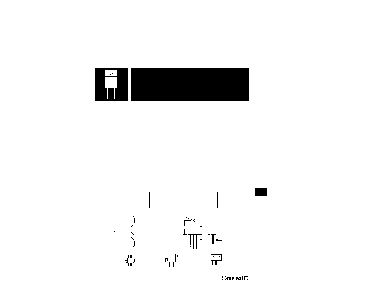
MAXIMUM RATINGS
@ 25∞C Unless Specified Otherwise
OM6508SA
OM6509SA
PART
I
C
(Cont.)
V
(BR)CES
V
CE (sat)
(Typ.)
T
f
(Typ.)
q
q
JC
P
D
T
J
NUMBER
@ 90∞C, A
V
V
ns
∞C/W
W
∞C
OM6508SA
5
500
2.8
400
3.8
35
150
OM6509SA
10
500
2.8
400
3.0
42
150
SCHEMATIC
.144 DIA.
.050
.040
.260
.249
.685
.665
.800
.790
.545
.535
.550
.510
.045
.035
.550
.530
.150 TYP.
.150 TYP.
.005
Collector
Emitter
1
2
3
C
E
G
Gate
MECHANICAL OUTLINE
Standard Products are supplied with glass feedthroughs. For ceramic feedthroughs, add the letter "C" to the part number. Example - OMXXXXCSA.
IGBTs are also available in Z-Tab, dual and quad pak styles - Please call the factory for more information.
PACKAGE OPTIONS
MOD PAK
Z-TAB
6 PIN SIP
PIN CONNECTION
Pin 1: Collector
Pin 2: Emitter
Pin 3: Gate
OM6508SA - OM6509SA
3.1
205 Craw
fo
rd St
re
et, Le
o
m
inster, MA 01
4
53 USA (50
8) 534
-57
76 FAX (508) 537-4246
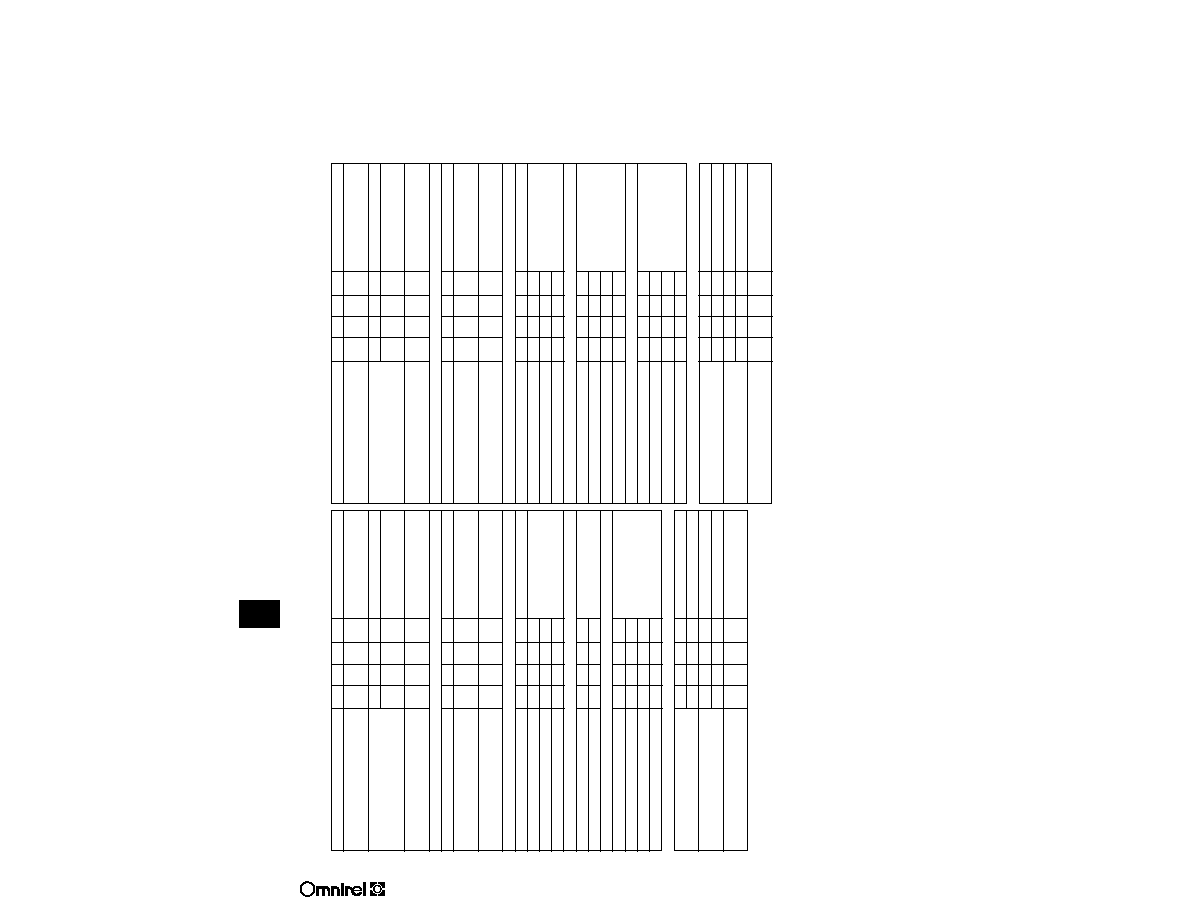
PRELIMINARY DATA: OM6508SA
IGBT CHARACTERISTICS
Parameter - OFF (see Note 1)
Min. Typ. Max. Units Test Conditions
V
(BR)CES
Collector Emitter
500
V
V
CE
= 0
Breakdown Voltage
I
C
= 250 µA
I
CES
Zero Gate Voltage
0.25
mA
V
CE
= Max. Rat., V
GE
= 0
Drain Current
1.0
mA
V
CE
= 0.8 Max. Rat., V
GE
= 0
T
C
= 125∞C
I
GES
Gate Emitter Leakage
±100
nA
V
GE
= ±20 V
Current
V
CE
= 0 V
Parameter - ON
V
GE(th)
Gate Threshold Voltage
2.0
4.0
V
V
CE
= V
GE
, I
C
= 250 µA
V
CE(sat)
Collector Emitter
3.0
V
V
GE
= 15 V, I
C
= 5 A
Saturation Voltage
T
C
= 25∞C
V
CE(sat)
Collector Emitter
2.8
3.0
V
V
GE
= 15 V, I
C
= 5 A
Saturation Voltage
T
C
= 100∞C
Dynamic
g
fs
Forward Transductance
2.0
S
V
CE
= 20 V, I
C
= 5 A
C
ies
Input Capacitance
260
pF
V
GE
= 0
C
oes
Output Capacitance
50
pF
V
CE
= 25 V
C
res
Reverse Transfer Capacitance
20
pF
f = 1 mHz
Switching-Resistive Load
T
d(on)
Turn-On Time
37
nS
V
CC
= 400 V, I
C
= 5 A
t
r
Rise Time
150
nS
V
GE
= 15 V, R
g
= 47
Switching-Inductive Load
t
r(Volt)
Off Voltage Rise Time
.35
µS
V
CEclamp
= 400 V, I
C
= 5 A
t
f
Fall Time
.81
µS
V
GE
= 15 V, R
g
= 100
t
cross
Cross-Over Time
1.2
µS
L = 0.1 mH, T
j
= 100∞C
E
off
Turn-Off Losses
.95
mJ
DIODE CHARACTERISTICS
V
f
Maximum Forward Voltage
1.5
V
I
F
= 8 A, T
C
= 25∞C
1.4
V
I
F
= 8 A, T
C
= 150∞C
I
r
Maximum Reverse Current
150
µA
V
R
= 600 V, T
C
= 25∞C
1.5
mA
V
R
= 480 V, T
C
= 125∞C
t
rr
Reverse Recovery Time
35
nS
I
F
= 1 A, d
i
/ d
t
= -15 A µ/S
V
R
= 30 V, T
j
= 25∞C
Note 1: Limited by diode I
r
characteristic.
PRELIMINARY DATA: OM6509SA
IGBT CHARACTERISTICS
Parameter - OFF (see Note 1)
Min. Typ. Max. Units Test Conditions
V
(BR)CES
Collector Emitter
500
V
V
CE
= 0
Breakdown Voltage
I
C
= 250 µA
I
CES
Zero Gate Voltage
0.25
mA
V
CE
= Max. Rat., V
GE
= 0
Drain Current
1.0
mA
V
CE
= 0.8 Max. Rat., V
GE
= 0
T
C
= 125∞C
I
GES
Gate Emitter Leakage
±100
nA
V
GE
= ±20 V
Current
V
CE
= 0 V
Parameter - ON
V
GE(th)
Gate Threshold Voltage
2.0
4.0
V
V
CE
= V
GE
, I
C
= 250 µA
V
CE(sat)
Collector Emitter
3.0
2.7
V
V
GE
= 15 V, I
C
= 10 A
Saturation Voltage
T
C
= 25∞C
V
CE(sat)
Collector Emitter
2.8
3.0
V
V
GE
= 15 V, I
C
= 10 A
Saturation Voltage
T
C
= 100∞C
Dynamic
g
fs
Forward Transductance
2.5
S
V
CE
= 20 V, I
C
= 10 A
C
ies
Input Capacitance
950
pF
V
GE
= 0
C
oes
Output Capacitance
140
pF
V
CE
= 25 V
C
res
Reverse Transfer Capacitance
80
pF
f = 1 mHz
Switching-Resistive Load
T
d(on)
Turn-On Time
150
nS
T
r
Rise Time
1000
nS
V
CC
= 400 V, I
C
= 10 A
T
d(off)
Turn-Off Delay Time
700
nS
V
GE
= 15 V, R
g
= 100
T
f
Fall Time
1500
nS
Switching-Inductive Load
T
d(off)
Turn-Off Delay Time
1.2
µS
V
CEclamp
= 350 V, I
C
= 10 A
t
f
Fall Time
1.5
µS
V
GE
= 15 V, R
g
= 100
t
cross
Cross-Over Time
2.0
µS
L = 180 µH, T
j
= 100∞C
E
off
Turn-Off Losses
4.0
mJ
DIODE CHARACTERISTICS
V
f
Maximum Forward Voltage
1.4
V
I
F
= 16 A, T
C
= 25∞C
1.5
V
I
F
= 16 A, T
C
= 150∞C
I
r
Maximum Reverse Current
500
µA
V
R
= 600 V, T
C
= 25∞C
3.0
mA
V
R
= 480 V, T
C
= 125∞C
t
rr
Reverse Recovery Time
35
nS
I
F
= 1 A, d
i
/ d
t
= -15 A µ/S
V
R
= 30 V, T
j
= 25∞C
Note 1: Limited by diode I
r
characteristic.