
3.5 - 97
3.5
4 11 R0
OM7603SM
Three Terminal, Adjustable Voltage, 1.0 Amp
Precision Negative Regulator In A Hermetic
Surface Mount Package
SURFACE MOUNT NEGATIVE ADJUSTABLE
VOLTAGE REGULATOR
FEATURES
∑ Hermetic Surface Mount Package
∑ Adjustable Output Voltage
∑ Built-In Thermal Overload Protection
∑ Short Circuit Current Limiting
∑ Product Is Available Hi-Rel Screened
∑ Electrically Similar To Industry Standard Type LM137
∑ Available Hi-Rel Screened
DESCRIPTION
This three terminal negative regulator is supplied in a hermetically sealed surface
mount package. All protective features are designed into the circuit, including thermal
shutdown, current limiting and safe-area control. With heat sinking, they can deliver
1.0 amp of output current. This unit features output voltages that can be trimmed
using external resistors, from -1.2 volts to -37 volts.
ABSOLUTE MAXIMUM RATINGS
@ 25∞C
Power Dissipation (P
d
) (Internally Limited). . . . . . . . . . . . . . . . . . . . . . . . . . . . . . . . . . 10 W
Input - Output Voltage Differential . . . . . . . . . . . . . . . . . . . . . . . . . . . . . . . . . . . . . . . . . 40 V
Operating Junction Temperature Range . . . . . . . . . . . . . . . . . . . . . . . . - 55∞C to + 150∞C
Storage Temperature Range . . . . . . . . . . . . . . . . . . . . . . . . . . . . . . . . . . - 65∞C to + 150∞C
Lead Temperature (Soldering 10 Seconds) . . . . . . . . . . . . . . . . . . . . . . . . . . . . . . . . 280∞C
Thermal Resistance: Junction-to-Case . . . . . . . . . . . . . . . . . . . . . . . . . . . . . . . . 13.5∞C/W
MECHANICAL OUTLINE
.450
SQ.
.300
4 PLCS.
.050
24 PLCS.
.305
SQ.
.02 x 45∞
.090
MAX.
.05 X 45∞
MAX. 3 PLCS.
.009 R.
28 PLCS.
.035
PIN 1
PIN 28
BOTTOM
TOP
SIDE
4
1
26
12
18
Pin Connection
Pin 1, 15 thru 28:
OUT
Pin 2, 3, 13, and 14: ADJ
Pin 4 thru 12:
IN
OM7603SM
3.5
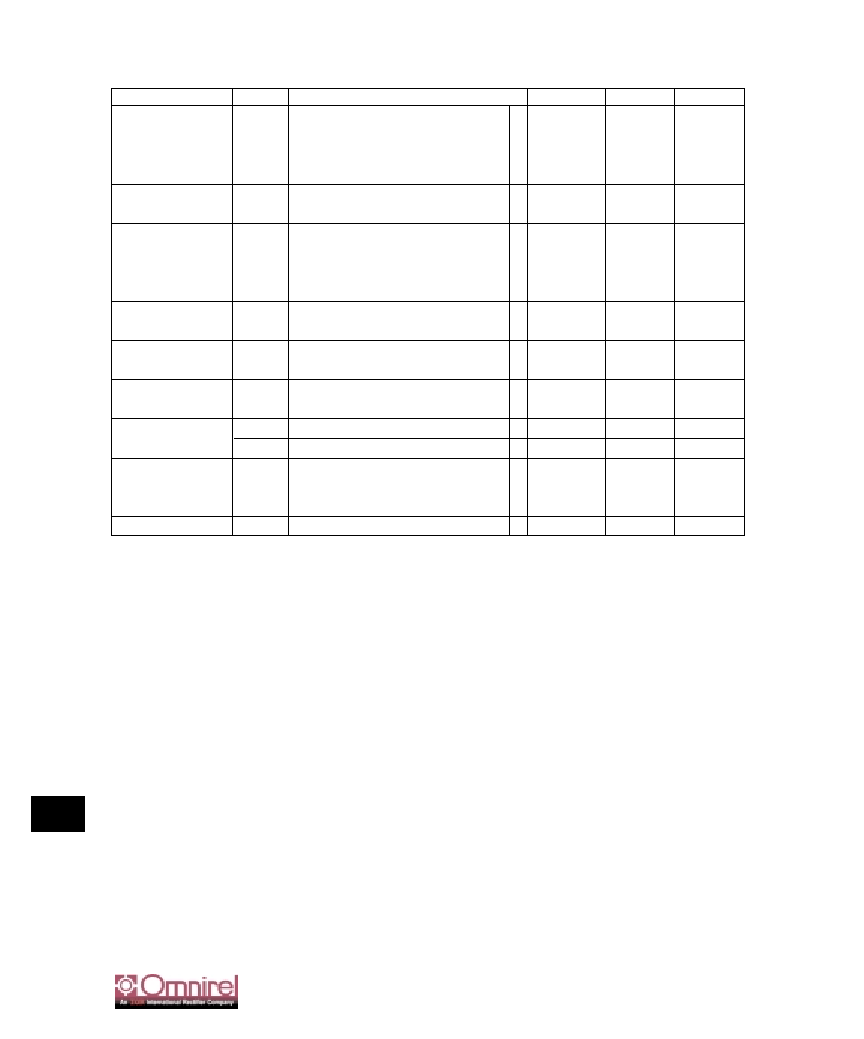
ELECTRICAL CHARACTERISTICS
-55∞C T
A
125∞C, I
L
= 8mA (unless otherwise specified)
Parameter
Symbol
Test Conditions
Min.Max.Unit
Reference Voltage
V
REF
V
DIFF
= 3.0V, T
A
= 25∞C
V
DIFF
= 3.0V
∑
-1.30
-1.20
V
V
DIFF
= 40V, T
A
= 25∞C
V
DIFF
= 40V
∑
-1.30
-1.20
Line Regulation
R
LINE
3.0 V
V
DIFF
40V, T
A
= 25∞C
-12
12
(Note 1)
3.0 V
V
DIFF
40V
∑
-25
25
mV
Load Regulation
R
LOAD
V
DIFF
= 5.0V, 8mA I
L
1.0A
∑
-30
30
(Note 1)
V
DIFF
= 12V, 8mA I
L
1.0A, T
A
= 25∞C
-30
30
mV
V
DIFF
= 40V, 8mA I
L
200mA, T
A
= 25∞C
-30
30
V
DIFF
= 40V, 8mA I
L
100mA
∑
-30
30
Thermal Regulation
V
RTH
V
IN
= -14.6V, I
L
= 1.0A
-16
16
mV
P
d
= 20 Watts, t = 20 ms, T
A
= 25∞C
Ripple Rejection
R
N
f = 120 Hz, V
OU
T = V
ref
∑
66
dB
(Note 2)
C
Adj
= 10 µF
Adjustment Pin Current
I
Adj
V
DIFF
= 3.0V
∑
100
V
DIFF
= 40V
∑
100
µA
Adjustment Pin
I
Adj
(Line)
3.0V
V
DIFF
40V
∑
-10
10
µA
Current Change
I
Adj
(Load)
V
DIFF
= 5V, 8mA I
L
1.0A
∑
-10
10
µA
Miminum Load Current
I
Lmin
V
DIFF
= 3.0V, V
OUT
= -1.4V (forced)
∑
10
V
DIFF
= 10V, V
OUT
= -1.4V (forced)
∑
10
mA
V
DIFF
= 40V, V
OUT
= -1.4V (forced)
∑
10
Current Limit (Note 2)
I
CL
V
DIFF
= 40V, T
A
= 25∞C
0.24
1.2
A
Notes:
1. Load and Line Regulation are specified at a constant junction temperature. Pulse testing with low duty cycle is used.
Changes in output voltage due to heating effects must be taken into account separately.
2. If not tested, shall be guaranteed to the specified limits.
3. The
∑
denotes the specifications which apply over the full operating temperature range.