3.5 - 109
3.5
4 11 R1
Supersedes 1 05 R0
FEATURES
∑ Surface Mount Hermetic Package
∑ Operates Down to 1V Dropout, 1.5V @ Max. Current
∑ .015% Typical Line Regulation
∑ .01% Typical Load Regulation
∑ 1% Reference Voltage
∑ Electrically Equivalent to LT1083, 84, 85 and 86
∑ Available Hi-Rel Screened
DESCRIPTION
These three terminal positive adjustable voltage regulators in surface mount package
are designed to provide 7.5A, 5A, 3A, and 1.5A with higher efficiency than
conventional voltage regulators. The devices are designed to operate to 1 Volt input
to output differential and the dropout voltage is specified as a function of load current.
These devices are ideally suited for Military applications where surface mount, small
size, hermeticity and high reliability are required.
ABSOLUTE MAXIMUM RATINGS
Input Voltage. . . . . . . . . . . . . . . . . . . . . . . . . . . . . . . . . . . . . . . . . . . . . . . . . . . . . . . . . . . 35 V
Operating Junction Temperature Range . . . . . . . . . . . . . . . . . . . . . . . - 55∞C to + 150∞C
Storage Temperature . . . . . . . . . . . . . . . . . . . . . . . . . . . . . . . . . . . . . . . . - 55∞C to + 150∞C
Output Current - OM7621NM. . . . . . . . . . . . . . . . . . . . . . . . . . . . . . . . . . . . . . . . . . . . 8.0 A
OM7622NM. . . . . . . . . . . . . . . . . . . . . . . . . . . . . . . . . . . . . . . . . . . . 5.5 A
OM7623NM. . . . . . . . . . . . . . . . . . . . . . . . . . . . . . . . . . . . . . . . . . . . 3.2 A
OM7624NM. . . . . . . . . . . . . . . . . . . . . . . . . . . . . . . . . . . . . . . . . . . . 1.5 A
a
OM7623NM
OM7624NM
OM7621NM
OM7622NM
SURFACE MOUNT LOW DROPOUT POSITIVE
ADJUSTABLE REGULATORS
Three Terminal Adjustable Low Dropout
7.5A, 5A, 3A, 1.5A Positive Voltage Regulators
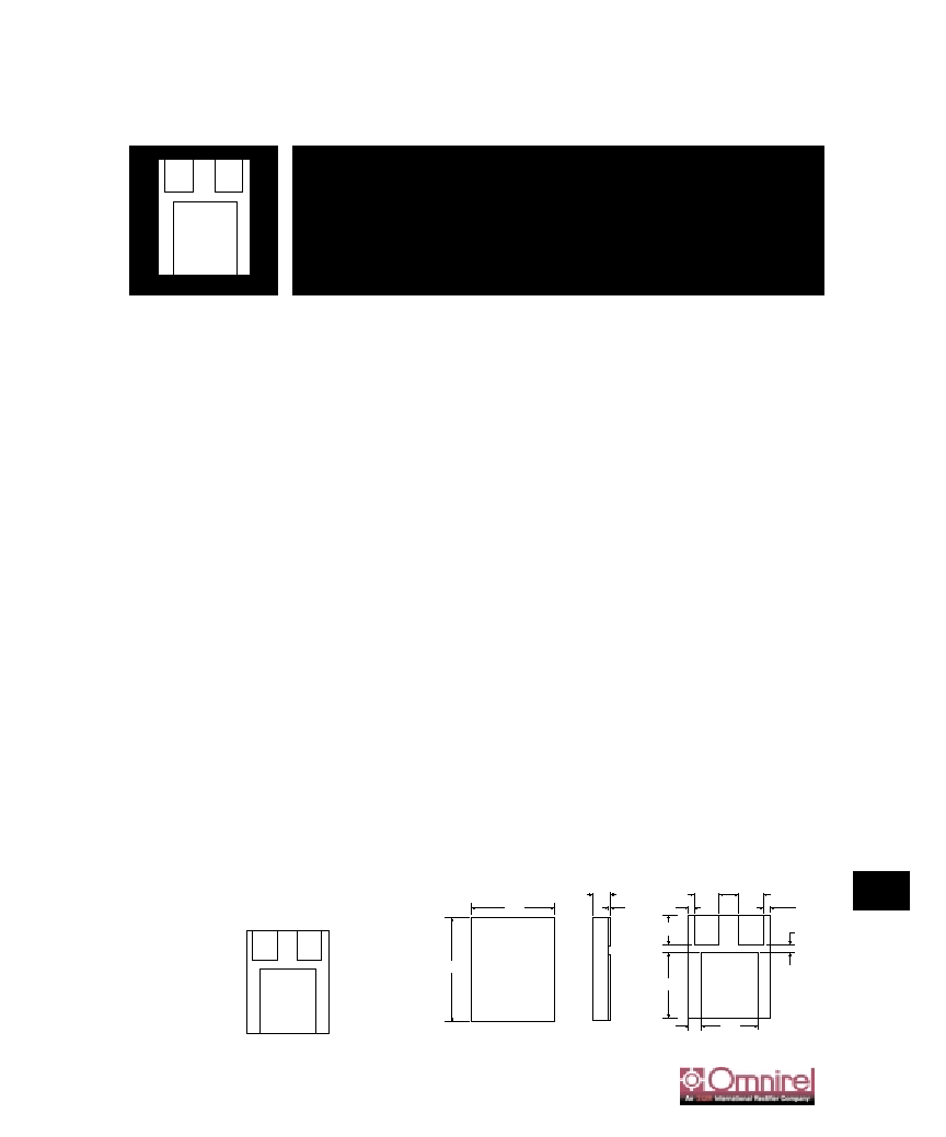
PIN CONNECTION
MECHANICAL OUTLINE
1
2
3
.500
.140
.415
.157
.015
.140
.140
.075
.075
.062
.375
.030
MIN.
TOP VIEW
SIDE VIEW
BOTTOM VIEW
.625
Pin 1: V
IN
Pin 2: Adjust
Pin 3: V
OUT
OM7621NM - OM7624NM
3.5
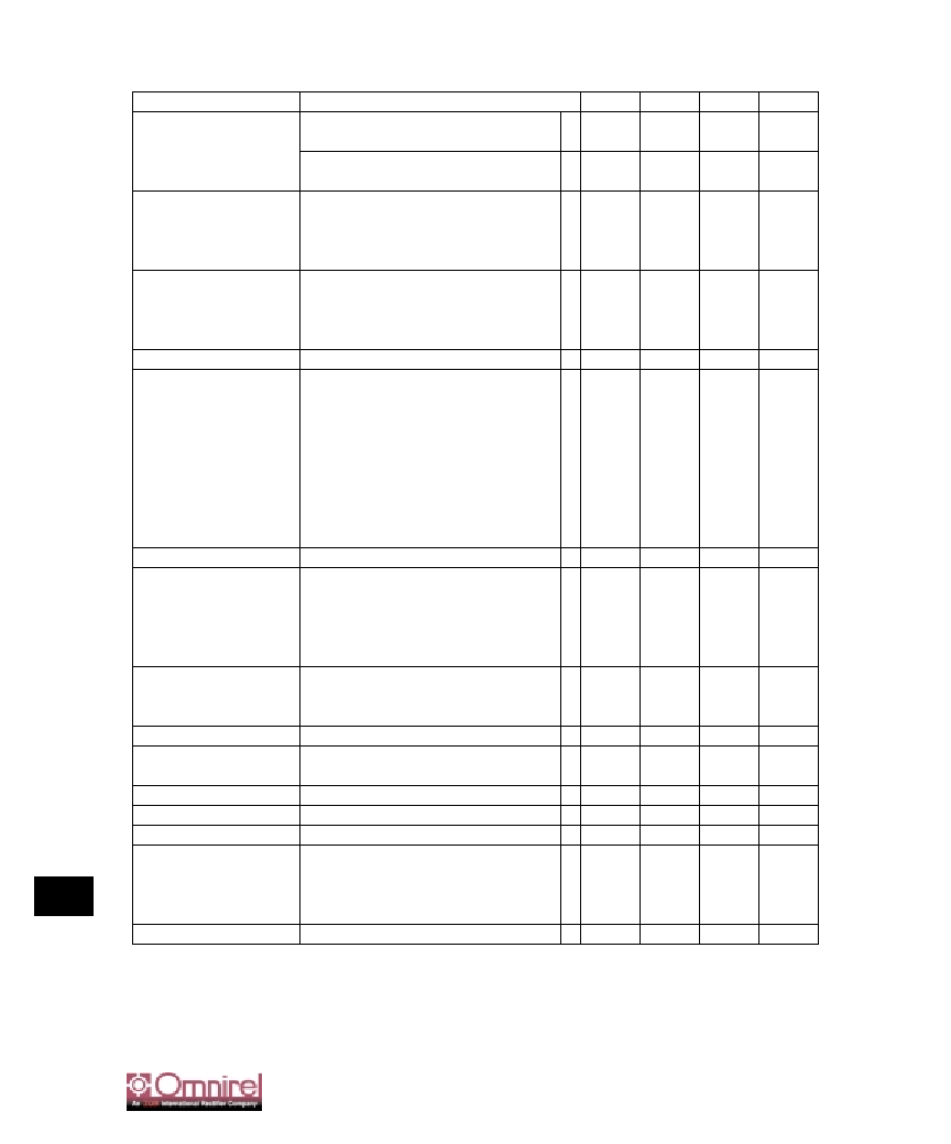
ELECTRICAL CHARACTERISTICS
T
J
= -55∞C to + 125∞C
Parameter
Conditions
Min.
Typ.
Max.
Units
Reference Voltage
I
OUT
= 10 mA, T
j
= 25∞C
(V
IN
- V
OUT
) = 3 V1.238
1.262
V
10mA I
OUT
I
FULL LOAD
1.5 V (V
IN
- V
OUT
) 25 V (Note 3)
∑
1.220
1.270
V
Line Regulation
I
LOAD
= 10 mA, 1.5 V (V
IN
- V
OUT
) 15 V, T
j
= 25∞C
0.25
%
%
15 V (V
IN
- V
OUT
) 35 V (Notes 1 & 2)
∑
0.55
%
Load Regulation
(V
IN
- V
OUT
) = 3 V
10 mA I
OUT
I
FULL LOAD
T
j
= 25∞C (Notes 1, 2, & 3)
0.9
%
∑
1.1
%
Dropout Voltage
V
REF
= 1%, I
OUT
= I
FULL LOAD
∑
1.5
V
Current Limit
OM7621NM
(V
IN
- V
OUT
) = 5 V
∑
8.0
A
(V
IN
- V
OUT
) = 25 V
∑
0.4
A
OM7622NM
(V
IN
- V
OUT
) = 5 V
∑
5.5
A
(V
IN
- V
OUT
) = 25 V
∑
0.3
A
OM7623NM
(V
IN
- V
OUT
) = 5 V
∑
3.2
A
(V
IN
- V
OUT
) = 25 V
∑
0.2
A
OM7624NM
(V
IN
- V
OUT
) = 5 V
∑
1.5
A
(V
IN
- V
OUT
) = 25 V
∑
0.08
A
Minimum Load Current
(V
IN
- V
OUT
) = 25 V
∑
20
mA
Thermal Regulation
T
A
= 25∞C, 30 ms pulse
OM7621NM
0.01
%/W
OM7622NM
.015
%/W
OM7623NM
0.02
%/W
OM7624NM
0.05
%/W
Ripple Rejection
f = 120 Hz
C
ADJ
= 25 µF Tantalum
I
OUT
- I
FULL LOAD
(V
IN
- V
OUT
) = 3 V60
dB
Adjust Pin Current
T
J
= 25∞C
80
µA
Adjust Pin Current Change
10mA I
OUT
I
FULL LOAD
1.5 V (V
IN
- V
OUT
) 25 V
∑
5
µA
Temperature Stability
-55∞C T
J
+150∞C
1.5
%
Long Term Stability
T
A
= 125∞C, 1000 Hrs.
1
%
Thermal Resistance
Junction-to-Case
OM7621NM
2.1
∞C/W
OM7622NM
3.1
∞C/W
OM7623NM
4.1
∞C/W
OM7624NM
5.3
∞C/W
Lead Temperature
5 Seconds at Case
225
∞C
Note 1: Load and line regulation are measured at a constant junction temperature by low duty cycle pulse testing.
Note 2: Line and load regulation are guaranteed up to the maximum power dissipation (OM7621/60W, OM7622/45W,
OM7623/30W, OM7624/15W). Power dissipation is determined by the input/output differential and the output
current. Guaranteed maximum power dissipation will not be available over the full input/output voltage range.
Note 3: I
FULL LOAD
curve is defined as the minimum value of current limit as a function of input to output voltage.
Note that power dissipation is only achievable over a limited range of input to output voltage.
Note 4: Dropout voltage is specified over the full output current range of the device.
The
∑
denotes the specifications which apply over the full operating temperature range.