 | –≠–ª–µ–∫—Ç—Ä–æ–Ω–Ω—ã–π –∫–æ–º–ø–æ–Ω–µ–Ω—Ç: OM9373SF | –°–∫–∞—á–∞—Ç—å:  PDF PDF  ZIP ZIP |
11/21/03
www.irf.com
1
FULL-FEATURED POWER MODULE OM9373SP
FOR DIRECT DRIVE OF
3-PHASE BRUSHLESS DC MOTOR
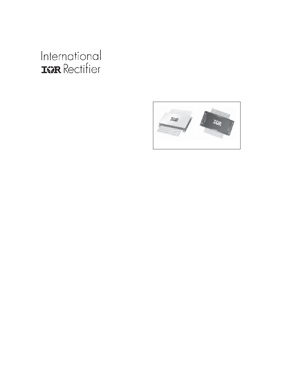
F-43 / MP3-43L Packages
Features:
n
Fully Integrated 3-Phase Brushless DC Motor
Control Subsystem includes Power Stage,
Non-Isolated Driver Stage and Controller Stage
n
MOSFET Output Stage
n
25A Average Phase Current with 80V
Maximum Bus Voltage
n
Internal Precision Current Sense Resistor
(6W Max. Dissipation)
n
Speed and Direction Control of Motor
n
Brake Input for Dynamic Braking of Motor
n
Overvoltage/Coast Input for Shutdown of
All Power Switches
n
Soft Start for Safe Motor Starting
n
Unique Hermetic or Plastic Ring Frame Power
Flatpacks
Hermetic (3.10" X 2.10" X 0.385")
Plastic Ring Frame (4.13" X 2.00" X 0.49")
Applications:
n
Fans and Pumps
n
Hoists
n
Actuator Systems
The OM9373 is one of a series of versatile, integrated
three-phase brushless DC motor controller/driver
subsystems housed in a 43 pin power flatpack. The
OM9373 is best used as a two quadrant speed
controller for controlling/driving fans, pumps, and
motors in applications which require small size.
Many integral control features provide the user much
flexibility in adapting the OM9373 to specific system
requirements.
MP3-43L
Description:
F-43
The small size of the complete subsystem is ideal for
aerospace, military, and high-end industrial applications.
Two package types provide a broad range of cost
and screening options to fit any application.
25A Push-Pull
3-Phase Brushless DC Motor
Controller / Driver Module
in a Power Flatpack
OM9373SF
OM9373
PD- 94705
OM9373
2
www.irf.com
* T
CASE
= 25∞C
* * T
CASE
= 25∞C, Maximum pulse width = 10 mS
Note 1: Logic Inputs: Direction, Hall Inputs (H1--- H3) Overvoltage - Coast, Speed, and Quad Select.
Note 2: The internal 5m
current sense resistor is limited to 6 Wdc power disipation. Other values are avaliable.
Please contact International Rectifier for more information.
Absolute Maximum Ratings
Parameter
Symbol
Value
Units
Motor Supply Voltage
V
m
80
Peak Motor Supply Voltage
V
m pk
100
Average Phase Output Current
I
o
25
A*
Peak Phase Output Current
I
om
50
Apeak **
Control Supply Voltage
V
cc
+18
Logic Input Voltage (Note 1)
-0.3 to +8.0
Reference Source Current
-30
mA
Error Amplifier Input Voltage Range
( EA1+ / EA1-)
-0.3 to +10
V
Error Amplifier Output Current
±8
mA
Spare Amplifier Input Voltage
( EA2+ / EA2-)
-0.3 to +10
V
Spare Amplifier Output Current
±8
mA
Current Sense Amplifier Input Voltage
(ISH / ISL)
-0.3 to +6.0
V
Current Sense Amplifier Output Current
Tachometer Output Current
PWM Input Voltage
-0.3 to +6.0
V
Operating Junction Temperature
-55 to 150
Storage Temperature Range
-65 to 150
∞C
Lead Soldering Temperature, 10s maximum, 0.125" from case
300
Package Isolation Voltage
600
Vrms
Power Switch Junction-to-Case Thermal Resistance
R
JC
0.35
∞C/W
V
±10
mA
V
Recommended Operating Conditions
( Tcase = 25∞C
)
Parameter
Symbol
Value
Units
Motor Power Supply Voltage
V
m
+48
V
Average Phase Output Current
With Internal Current Sense Resistor
( Note2 )
I
o
25
A
Each Power Switch
Control Supply Voltage
V
cc
15+10%
Logic Low Input Voltage (maximum)
V
il
0.8
V
Logic High Input Voltage (minimum)
V
ih
2.0
www.irf.com
3
OM9373
Electrical Characteristics
Parameter
Symbol
Test Conditions (Note 1)
Min.
Typ. Max. Units
Power Output Section
Zero Gate Voltage Drain Current
I
dss
V
ds
= 80Vdc, Vgs = 0V
-
-
250
µ
Drain-to-Source On-Resistance
R
ds(on)
I
d
= 35A, Vgs
= 10V
( Note 4 )
-
-
0.024 Ohms
Gate Body Leakage Current
I
gssr
V
gs
= 20V
dc
, V
ds
= 0V
-
-
100
nA
Diode Forward Voltage
V
f
I
S
= 35A
-
-
0.9
V
Diode Reverse Recovery Time
t
rr
I
S
= 25A, di/dt = -100A/
µ
sec, V
GS
= 0V
-
-
200
nS
Control Section
Control Supply Current
I
cc
V
CC
over operating range
-
-
100
mA
Control Turn-On Threshold
9.45
-
-
Driver Turn-On Threshold
13
-
-
Reference Section
Output Voltage
4.9
5.0
5.1
Output Voltage
4.7
5.0
5.3
Output Current
Io
-
-
30
mA
Load Regulation
I
LOAD
= 0mA to -20mA
-40
-5.0
-
mV
Short Circuit Current
I
sc
T
C
over operating range
50
100
150
mA
Error / Spare Amplifiers Section
EA1 / EA2 Input Offset Current
I
os
V(pin 2) = V(pin 4) = 0V,
-30
-3.0
0
V(pin 3) = V(pin 6) = 0V
EA1 / EA2 Input Bias Current
I
in
V(pin 2) = V(pin 4) = 0V,
-50
-45
0
V(pin 3) = V(pin 6) = 0V
Input Offset Voltage
V
os
0V < Vcommon-mode < 3.0V
-
-
7.0
mV
Amplifier Output Voltage Range
-
0
-
6.0
V
PWM Comparator Section
PWM Input Current
I
in
V(pin 9) = 2.5V
0
3.0
30
µ
Current-Sense Amplifier Section
ISH / ISL Input Current
I
in
V(pin 12) = V(pin 13) = 0V,
-850
-320
0
Input Offset Current
I
os
V(pin 12) = V(pin 13) = 0V,
-
±2.0
±12
Peak Current Threshold Voltage
V
pk
V(pin 12) = 0V, V(pin 13) Varied to
0.14
0.20
0.26
Over Current Threshold Voltage
V
oc
Threshold
0.26
0.30
0.36
V
ISH / ISL Input Voltage Range
-
( Note 2 )
-1.0
-
2.0
Amplifier Voltage Gain
A
V
V(pin 12) = 0.3V, V(pin 13) = 0.5V to 0.7V
1.75
1.95
2.15
V/V
Amplifier Level Shift
-
V(pin 12) = V(pin 13) = 0.3V
2.4
2.5
2.65
V
µ
V
cc
(+)
T
C
over operating range
V
V
ref
T
C
over operating range
V
nA
OM9373
4
www.irf.com
1. All parameters specified for Ta = 25∞C, Vcc = 15Vdc, Rosc= 75K
(to Vref), Cosc = 1800pF, and all Phase Outputs unloaded (Ta-Tj).
All negative currents shown are sourced by (flow from) the pin under test.
2. Either ISH or ISL may be driven over the range shown.
3. Bold parameters tested over temperature range.
4. Pulse Test: Pulse Width
£
300
µ
Sec,Duty Cycle
£
2%.
Specification Notes:
Electrical Characteristics -
Continued
Parameter
Symbol Test Conditions (Note 1) Min.
Typ. Max. Units
Logic Input Section
H1, H2, H3 Low Voltage Threshold
V
il
0.8
1.0
1.2
H1, H2, H3 High Voltage Threshold
V
ih
1.6
1.9
2.0
H1, H2, H3 Input Current
I
in
TC over operating range,
-400
-250
-120
µ
V(pin 20, 21, or 22) = 0Vdc
Quad Select / Direction Threshold Voltage
V
th
T
C
over operating range
0.8
1.4
2.0
V
Quad Select Voltage Hysteresis
-
70
-
mV
Direction Voltage Hysteresis
-
0.6
-
V
Quad Select Input Current
-30
50
150
Direction Input Current
-30
-1.0
30
Overvoltage / Coast Input Section
Overvoltage / Coast Inhibit Threshold Voltage
1.65
1.75
1.85
Overvoltage / Coast Restart Threshold Voltage
T
C
over operating range
1.55
1.65
1.75
V
Overvoltage / Coast Hysteresis Voltage
V
h
0.05
0.10
0.15
Overvoltage / Coast Restart Input Current
I
in
-10
-1.0
0
µ
Soft-Start Section
Soft-Start Pull-Up Current
I
p
V(pin 18) = 0V
-16
-10
-5.0
µ
Soft-Start Discharge Current
I
d
V(pin 18) = 2.5V
0.1
0.4
3.0
mA
Soft-Start Reset Threshold Voltage
V
th
0.1
0.2
0.3
V
Tachometer/Brake Section
Tachometer Output High Level
V
oh
T
c
over operating range
4.7
5.0
5.3
Tachometer Output Low Level
V
ol
(pin15) 10K
to 2.5V
-
-
0.2
Tachometer On-Time
t
on
85
100
140
µ
S
Tachometer On-Time Variation
-
T
C
over operating range
-
0.1
-
%
Brake/Tach Timing Input Current
I
in
V(pin 16) = 0V
-4.0
-1.9
-
mA
Brake/Tach Timing Threshold Voltage
V
th
T
C
over operating range
0.8
1.0
1.2
Voltage Hysteresis
V
h
-
0.09
-
Speed Input Threshold Voltage
V
th
T
C
over operating range
220
257
290
mV
Speed Input Current
I
in
-30
-5.0
30
µ
A
Oscillator Section
Oscillator Frequency
f
o
Measured at pin 10
13.5
14.8
20
KHz
V
T
C
over operating range
V
th
V
V
l
in
µ
V
h
www.irf.com
5
OM9373
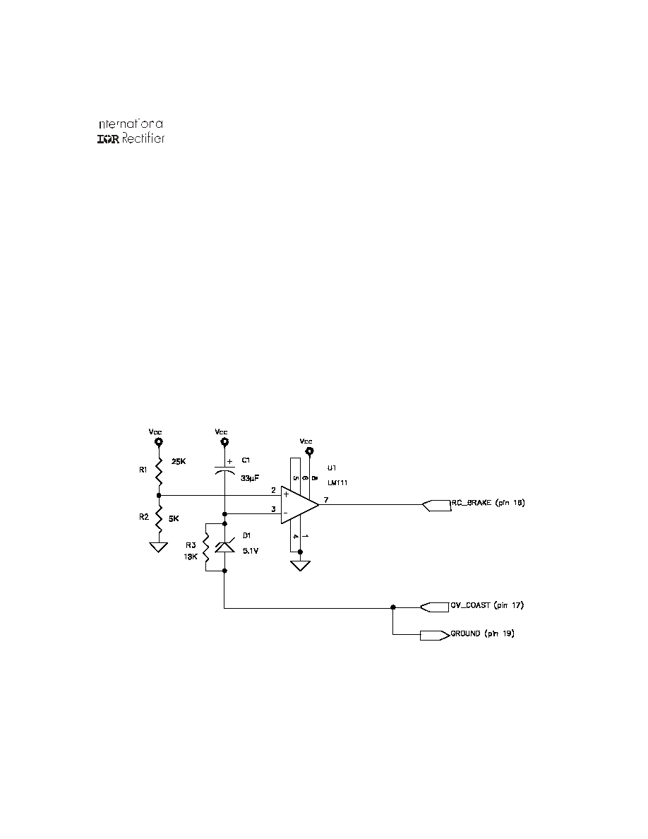
The OM9373 3-phase brushless DC motor controller/
driver is designed to drive fractional to integral
horsepower motors. To ensure proper operation, it is
necessary to ensure that the high-side bootstrap
capcitors are charged during initial start-up. However,
the method(s) used to ensure this may be dependant
upon the application. For example, some applications
may only require that OV_COAST (pin 17) be
connected to ground, either via a hardwire connection
or via a switch (Enable/Disable), before applying Vcc.
When Vcc is applied, the controller/driver is forced
into brake mode for approximately 200
µ
s (all high-
side drivers are disabled and all low-side drivers are
enabled).
APPLICATIONS
Start-Up Conditions
Fig 1: Optional Start-Up Circuit
This may not be adequate for other applications;
while maintaining a constant speed command,(above
zero),the RC_BRAKE (pin 16) may have to be
momentarily connected to ground via a switch,
either manually or electronically (ref. Figure 1).
Note that with the component values shown in
Figure 1, RC_BRAKE is pulled for low for approximately
300ms after applying Vcc at pin 1.