
3.4
3.4 - 1
4 11 R1
Supersedes 2 05 R0
FEATURES
∑ Available In Isolated Standard TO-3, "Copper Slug" TO-3 And
Power DIP Packages
∑ 5 Amp Peak Output Current
∑ Power Supplies to Ī40V
∑ FET Input
∑ Dual Configuration
∑ Available Screened to MIL-STD-883
DESCRIPTION
The OMA2541 is a high performance dual power operational amplifier capable of
operation from power supplies up to Ī40V and continuous output current up to 5A.
This device is ideally suited for Military motor driver, servo amplifiers, bridge amplifier,
synchro/resolver exertation as well as other power management driver applications.
Internal circuitry limits output current to approximately 6 Amps. All products are
available with Hi-Rel screening.
ABSOLUTE MAXIMUM RATINGS
@ 25įC
Supply Voltage, +V
S
to -V
S
. . . . . . . . . . . . . . . . . . . . . . . . . . . . . . . . . . . . . . . . . . . . 80V
Output Current, Continuous . . . . . . . . . . . . . . . . . . . . . . . . . . . . . . . . . . . . . . . . . . . . . 5A
Power Dissipation, Internal . . . . . . . . . . . . . . . . . . . . . . . . . . . . . . . . . . . . . . . . . . . 125W
Operating Temperature Range . . . . . . . . . . . . . . . . . . . . . . . . . . . . . . . -55įC to 125įC
Storage Temperature Range . . . . . . . . . . . . . . . . . . . . . . . . . . . . . . . . . -55įC to 150įC
Maximum Junction Temperature . . . . . . . . . . . . . . . . . . . . . . . . . . . . . . . . . . . . . . 175įC
Lead Temperature (10 Sec. Soldering) . . . . . . . . . . . . . . . . . . . . . . . . . . . . . . . . 300įC
8-Pin TO-3 And 12-Pin DIP, Dual 5 Amp
Operational Amplifier
DUAL HIGH POWER OPERATIONAL AMPLIFIER
OMA2541SKC
OMA2541SK
OMA2541SD
SCHEMATIC
PIN CONNECTION
TOP VIEW D-12
TOP VIEW TO-3
Out
B
+V
S
-V
S
-In
A
Out
A
+In
B
1
2
3
4
5
6
7
8
+
+
-
-
A
B
-In
B
+In
A
Output
(5,1)
-In
-V
S
+In
+V
S
+IN
B
-IN
B
-V
S
+IN
A
-IN
A
NC
OUT
B
NC
NC
+V
S
NC
Pin 1
Designation
∑

3.4
3.4 - 2
OMA2541SK OMA2541SKC OMA2541SD
ELECTRICAL CHARACTERISTICS
(T
C
= 25įC; V
S
= Ī34 V
DC
unless otherwise noted.)
Parameter
Conditions
Min.
Typ.
Max.
Units
Input Offset Voltage
V
OS
Ī.01
Ī2
mV
vs Temperature
-25įC to +125įC
Ī15
Ī30
ĶV/įC
vs Temperature
-55įC to -25įC
Ī20
Ī40
ĶV/įC
vs Supply Voltage
V
S
= Ī10V to Ī V
MAX
Ī2.5
Ī10
ĶV/V
vs Power
Ī20
Ī60
ĶV/W
Input Bias Current
I
B
4
50
pA
Input Offset Current
Ī1
Ī30
pA
I
OS
Specified Temperature Range
Ī5
Ī20
nA
Input Characteristics
Common-Mode Voltage Range
-55įC to +85įC
Ī(
oe
V
S
oe
- 6)
Ī(
oe
V
S
oe
- 3)
V
+85įC to +125įC
Ī(
oe
V
S
oe
- 6.5)
Ī(
oe
V
S
oe
- 3.2)
V
Common-Mode Rejection
V
CM
= Ī(
oe
V
S
oe
- 6V)
113
dB
V
CM
= Ī22V
95
dB
Input Capacitance*
5
pF
Input Capacitance, DC*
1
T
Gain Characteristics
Open Loop Gain at 10Hz
R
L
= 10k
90
97
dB
Gain Bandwidth Product*
1.6
MHz
Output
Voltage Swing
I
O
= 5A, Continuous
Ī(
oe
V
S
oe
- 5.5)
Ī(
oe
V
S
oe
- 4.5)
V
I
O
= 2A
Ī(
oe
V
S
oe
- 4.5)
Ī(
oe
V
S
oe
- 3.6)
V
I
O
= 0.5A
Ī(
oe
V
S
oe
- 4)
Ī(
oe
V
S
oe
- 3.2)
V
Current Peak
9
10
A
AC Performance
Slew Rate
6
10
V/ĶS
Power Bandwidth*
R
L
= 8 , V
O
= 20V
rms
55
KHz
Setting Time to 0.1%*
2V Step
2
ĶS
Capacitive Load*
Specified Temperature Range, G =1
3.3
A
Specified Temperature Range, G >10
SOA
Phase Margin*
Specified Temperature Range, R
L
= 8
40
Degrees
Power Supply
Power Supply Voltage, ĪV
S
Ī10
Ī35
Ī40
V
Current Quiescent -
50
60
mA
Both Amplifiers
Specified Temperature Range
60
70
mA
Thermal Resistance
Standard
Copper Slug
Power
Maximum
Conditions
TO-3
TO-3
DIP
Units
q
JC
(Junction-to-Case)
Both Amplifiers(2), AC Output f > 60Hz
1.0
.8
.65
įC/W
Both Amplifiers(2), DC Output
1.2
1.0
.80
įC/W
One Amplifier, AC Output f > 60Hz
1.5
1.2
1.00
įC/W
One Amplifier, DC Output
1.9
1.5
1.15
įC/W
q
JA
(Junction-to-Ambient)
No Heat Sink
30
30
30
įC/W
NOTES: (1) Input bias and offset current approximately doubles for every 10įC increase in temperature.
(2) Assumes equal dissipation in both amplifiers.
(
*
)
Guaranteed - not tested 100%.

3.4
3.4 - 3
OMA2541SK OMA2541SKC OMA2541SD
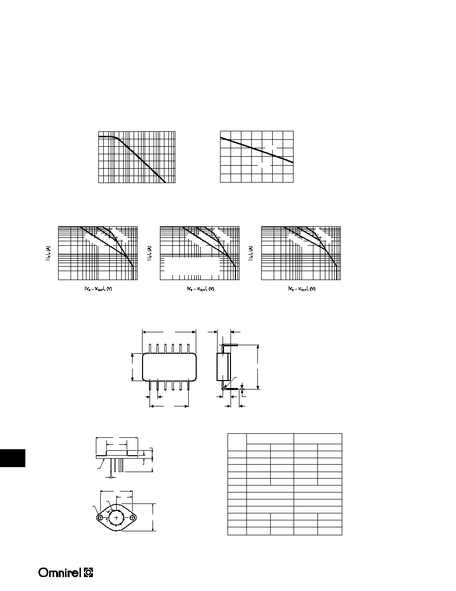
TYPICAL PERFORMANCE CURVES
T
A
= +25įC, V
S
= ĪV
DC
unless otherwise noted
110
1
Voltage Gian, (dB)
Frequency, (Hz)
Open-Loop Gain and
Phase VS Frequency
100
90
80
70
60
50
40
30
20
10
0
-10
10
100
1k
10k
100k
1M
10M
100
Input Bias Current, (nA)
10
1
0.1
0.01
0.001
-25
Junction Temperature, (Cį)
Input Bias Current
VS Temperature
0
25
50
75
100
125
1.3
Normalized I
Q
20
+V
S
+
-V
S
, (V)
Normalized Quiescent Current VS
Total Power Supply Voltage
1.2
1.1
1.0
0.9
0.8
0.7
0.6
30
40
50
60
70
80
90
1k
Voltage Noise Density,
Frequency, (Hz)
Voltage Noise Density
VS Frequency
1
100
10
10
100
1k
10k
100k
T
C
= 25įC
T
C
= -25įC
T
C
= 125įC
1
6
5
4
3
2
1
0
2
3
4
5
6
7
8
9
10
Ī
V
S
-
V
OUT
, (V)
Output Voltage Swing
VS Output Current
I
OUT
,
(A)
-V
S
-
V
O
(+V
S
) - V
O
10
THD +
Noise, (%)
Frequency, (Hz)
Total Harmonic Distortion
VS Frequency
10
100
1k
10k
100k
1.0
0.1
0.01
0.001
P
O
= 100mW
P
O
= 5W
P
O
= 50W
Z
L
= 3.3nF
Z
L
= 3.3nF
Phase
Gain
3.4
205 Crawford Street, Leominster, MA 01453 USA (508) 534-5776 FAX (508) 537-4246
OMA2541SK OMA2541SKC OMA2541SD
120
CMRR, (dB)
Frequency, (Hz)
Typical Common-Mode Rejection
VS Frequency (Case Dependent)
10
110
100
80
70
60
50
90
100
1k
10k
100k
1M
12
Output Current, (A)
Case Temperature, (įC)
Typical Output Current
VS Temperature (Case Dependent)
-50
10
8
6
4
2
0
-25
0
25
50
75
100 125
I
OUT
+
I
OUT
-
10
Safe Operating Area
OMA2541SKC
T
C
= 25įC
1.0
0.1
1
10
100
T
C
= 85įC
T
C
= 125įC
10
Safe Operating Area
OMA2541SK
T
C
= 25įC
1.0
0.1
1
10
100
T
C
= 85įC
T
C
= 125įC
*
* Depending on temperature maximum
output may be restricted by internal
current limit. See output current
specifications and typical curves.
10
Safe Operating Area
OMA2541SD/SDZ
Copper Slug TO-3
Standard TO-3
Power DIP
T
C
= 25įC
1.0
0.1
1
10
100
T
C
= 125įC
T
C
= 85įC
MECHANICAL OUTLINE
H
1
2 3
4
5
6
7
8
F
J
G
Q
R
K
A
B
C
E
D
SEATING
PLANE
INCHES
MILLIMETERS
DIM
MIN
MAX
MIN
MAX
A
1.510
1.550
38.35
39.37
B
.745
.770
18.92
19.56
C
.260
.300
6.60
7.62
D
.038
.042
0.97
1.07
E
.080
.105
2.03
2.67
F
40į BASIC
40į BASIC
G
.500 BASIC
12.7 BASIC
H
1.186 BASIC
30.12 BASIC
J
.593 BASIC
15.06 BASIC
K
.400
.500
10.16
12.70
Q
.151
.161
3.84
4.09
R
.980
1.020
24.89
25.91
Note: Leads in true position within 0.010" (0.25mm) R at MMC at seating plane.
Pin numbers shown for reference only. Numbers may not be marked on package.
.150
.030 DIA.
.040 R.
MIN.
.180 MIN.
.900
.260
MAX.
.150
1.050
.540
.750
D-12
TO-3-8