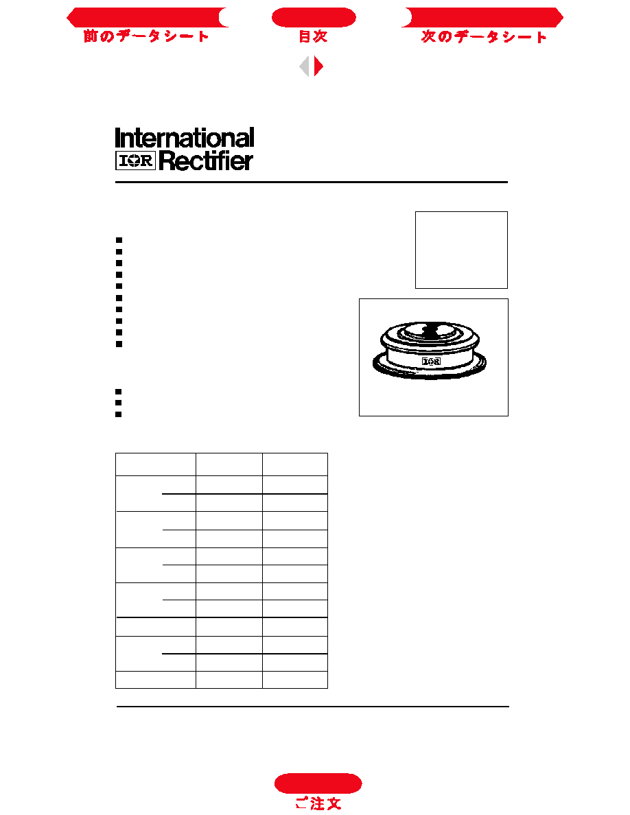
SD303C..C SERIES
FAST RECOVERY DIODES
Hockey Puk Version
350A
D-655
Bulletin I2066/B
Features
High power FAST recovery diode series
1.0 to 2.0 µs recovery time
High voltage ratings up to 2500V
High current capability
Optimized turn on and turn off characteristics
Low forward recovery
Fast and soft reverse recovery
Press-puk encapsulation
Case style conform to JEDEC DO-200AA
Maximum junction temperature 125∞C
Typical Applications
Snubber diode for GTO
High voltage free-wheeling diode
Fast recovery rectifier applications
Major Ratings and Characteristics
I
F(AV)
350
A
@ T
hs
55
∞C
I
F(RMS)
550
A
@ T
hs
25
∞C
I
FSM
@
50Hz
5770
A
@ 60Hz
6040
A
I
2
t
@
50Hz
166
KA
2
s
@ 60Hz
152
KA
2
s
V
RRM
range
400 to 2500
V
t
rr
range
1.0 to 2.0
µs
@ T
J
25
∞C
T
J
- 40 to 125
∞C
Parameters
SD303C..C
Units
case style DO-200AA
Next Data Sheet
Index
Previous Datasheet
To Order

SD303C..C Series
2222222222222
12
D-656
Code
(
µ
s)
(A)
(A/
µ
s)
(V)
(
µ
s)
(
µ
C)
(A)
Test conditions
Max. values @ T
J
= 125
∞C
Recovery Characteristics
typical t
rr
I
pk
di/dt
V
r
t
rr
Q
rr
I
rr
@ 25% I
RRM
Square Pulse
@ 25% I
RRM
T
J
= 25
o
C
S10
1.0
2.4
52
33
S15
1.5
750
25
-30
2.9
90
44
S20
2.0
3.2
107
46
Voltage
V
RRM
max. repetitive
V
RSM
, maximum non-
I
RRM
max.
Type number
Code
peak and off-state voltage
repetitive peak voltage
T
J
= 125∞C
V
V
mA
04
400
500
SD303C..S10C
08
800
900
10
1000
1100
12
1200
1300
SD303C..S15C
14
1400
1500
16
1600
1700
20
2000
2100
25
2500
2600
ELECTRICAL SPECIFICATIONS
Voltage Ratings
SD303C..S20C
Parameter
SD303C..C
Units
Conditions
I
F(AV)
Max. average forward current
350(175)
A
180∞ conduction, half sine wave.
@ Heatsink temperature
55(75)
∞C
Double side (single side) cooled
I
F(RMS)
Max. RMS current
550
A
@ 25∞C heatsink temperature double side cooled
I
FSM
Max. peak, one-cycle
5770
t = 10ms
No voltage
non-repetitive forward current
6040
t = 8.3ms
reapplied
4850
t = 10ms
100% V
RRM
5080
t = 8.3ms
reapplied
Sinusoidal half wave,
I
2
t
Maximum I
2
t for fusing
166
t = 10ms
No voltage
Initial T
J
= T
J
max.
152
t = 8.3ms
reapplied
117
t = 10ms
100% V
RRM
107
t = 8.3ms
reapplied
I
2
t
Maximum I
2
t for fusing
1660
KA
2
s
t = 0.1 to 10ms, no voltage reapplied
V
F(TO)1
Low level of threshold voltage
1.14
(16.7% x
x I
F(AV)
< I <
x I
F(AV)
), T
J
= T
J
max.
V
F(TO)2
High level of threshold voltage
1.63
(I >
x I
F(AV)
), T
J
= T
J
max.
r
f1
Low level of forward slope resistance
1.14
(16.7% x
x I
F(AV)
< I <
x I
F(AV)
), T
J
= T
J
max.
r
f2
High level of forward slope resistance
0.77
(I >
x I
F(AV)
), T
J
= T
J
max.
V
FM
Max. forward voltage
2.26
V
I
pk
= 1100A, T
J
= 25∞C, t
p
= 10ms sinusoidal wave
Forward Conduction
KA
2
s
A
m
V
35
Next Data Sheet
Index
Previous Datasheet
To Order
SD303C..C Series
D-659
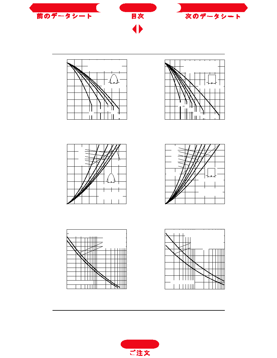
Fig. 3 - Current Ratings Characteristics
Fig. 4 - Current Ratings Characteristics
Fig. 6 - Forward Power Loss Characteristics
Fig. 5 - Forward Power Loss Characteristics
Fig. 7 - Maximum Non-repetitive Surge Current
Single and Double Side Cooled
Fig. 8 - Maximum Non-repetitive Surge Current
Single and Double Side Cooled
To Order
Next Data Sheet
Index
Previous Datasheet

SD303C..C Series
D-660
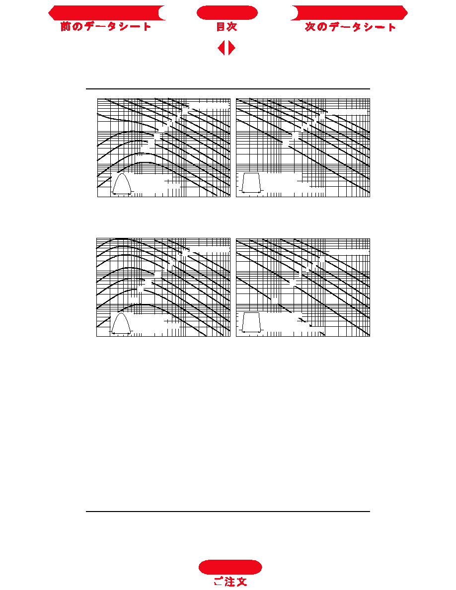
Fig. 9 - Forward Voltage Drop Characteristics
Fig. 10 - Thermal Impedance Z
thJ-hs
Characteristic
Fig. 11 - Typical Forward Recovery Characteristics
Fig. 12 - Recovery Time Characteristics
Fig. 13 - Recovery Charge Characteristics
Fig. 14 - Recovery Current Characteristics
To Order
Next Data Sheet
Index
Previous Datasheet

SD303C..C Series
D-661
Fig. 16 - Recovery Charge Characteristics
Fig. 15 - Recovery Time Characteristics
Fig. 17 - Recovery Current Characteristics
Fig. 18 - Recovery Time Characteristics
Fig. 19 - Recovery Charge Characteristics
Fig. 20 - Recovery Current Characteristics
Fig. 21 - Maximum Total Energy Loss Per Pulse Characteristics
To Order
Next Data Sheet
Index
Previous Datasheet
SD303C..C Series
D-662
Fig. 22 - Maximum Total Energy Loss Per Pulse Characteristics
Fig. 23 - Maximum Total Energy Loss Per Pulse Characteristics
To Order
Next Data Sheet
Index
Previous Datasheet
SD303C..C Series
23
D-657
3333
T
J
Max. operating temperature range
-40 to 125
T
stg
Max. storage temperature range
-40 to 150
R
thJ-hs
Max. thermal resistance,
0.16
DC operation single side cooled
junction to heatsink
0.08
DC operation double side cooled
F
Mounting force, ± 10%
4900
N
(500)
(Kg)
wt
Approximate weight
70
g
Case style
DO-200AA
See Outline Table
Parameter
SD303C..C
Units
Conditions
Thermal and Mechanical Specifications
R
thJ-hs
Conduction
(The following table shows the increment of thermal resistence R
thJ-hs
when devices operate at different conduction angles than DC)
∞C
K/W
1
-
Diode
2
-
Essential part number
3
-
3 = Fast recovery
4
-
C = Ceramic Puk
5
-
Voltage code: Code x 100 = V
RRM
(see Voltage Ratings table)
6
-
t
rr
code (see Recovery Characteristics table)
7
-
C = Puk Case DO-200AA
Ordering Information Table
5
1
2
3
4
SD
30
3
C
25 S20
C
7
6
Device Code
Sinusoidal conduction
Rectangular conduction
Conduction angle
Units
Conditions
Single Side Double Side
Single Side Double Side
180∞
0.010
0.011
0.008
0.008
120∞
0.012
0.013
0.013
0.013
90∞
0.016
0.016
0.018
0.018
K/W
T
J
= T
J
max.
60∞
0.024
0.024
0.025
0.025
30∞
0.042
0.042
0.042
0.042
To Order
Next Data Sheet
Index
Previous Datasheet
SD303C..C Series
2222222222222
12
D-658
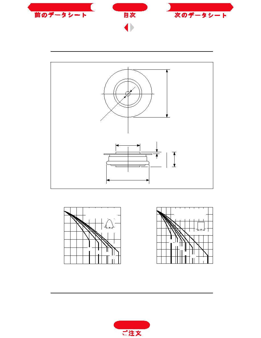
Outline Table
Fig. 1 - Current Ratings Characteristics
Fig. 2 - Current Ratings Characteristics
Case Style DO-200AA
All dimensions in millimeters (inches)
0.3 (0.01) MIN.
BOTH ENDS
4
2
(
1
.
6
5
)
D
I
A
.
M
A
X
.
38 (1.50) DIA. MAX.
TWO PLACES
3.5(0.14) ± 0.1(0.004) DIA. NOM.x
1.8 (0.07) DEEP MIN. BOTH ENDS
19(0.75) DIA. MAX.
1
4
.
4
(
0
.
5
7
)
1
3
.
7
(
0
.
5
4
)
To Order
Next Data Sheet
Index
Previous Datasheet