1
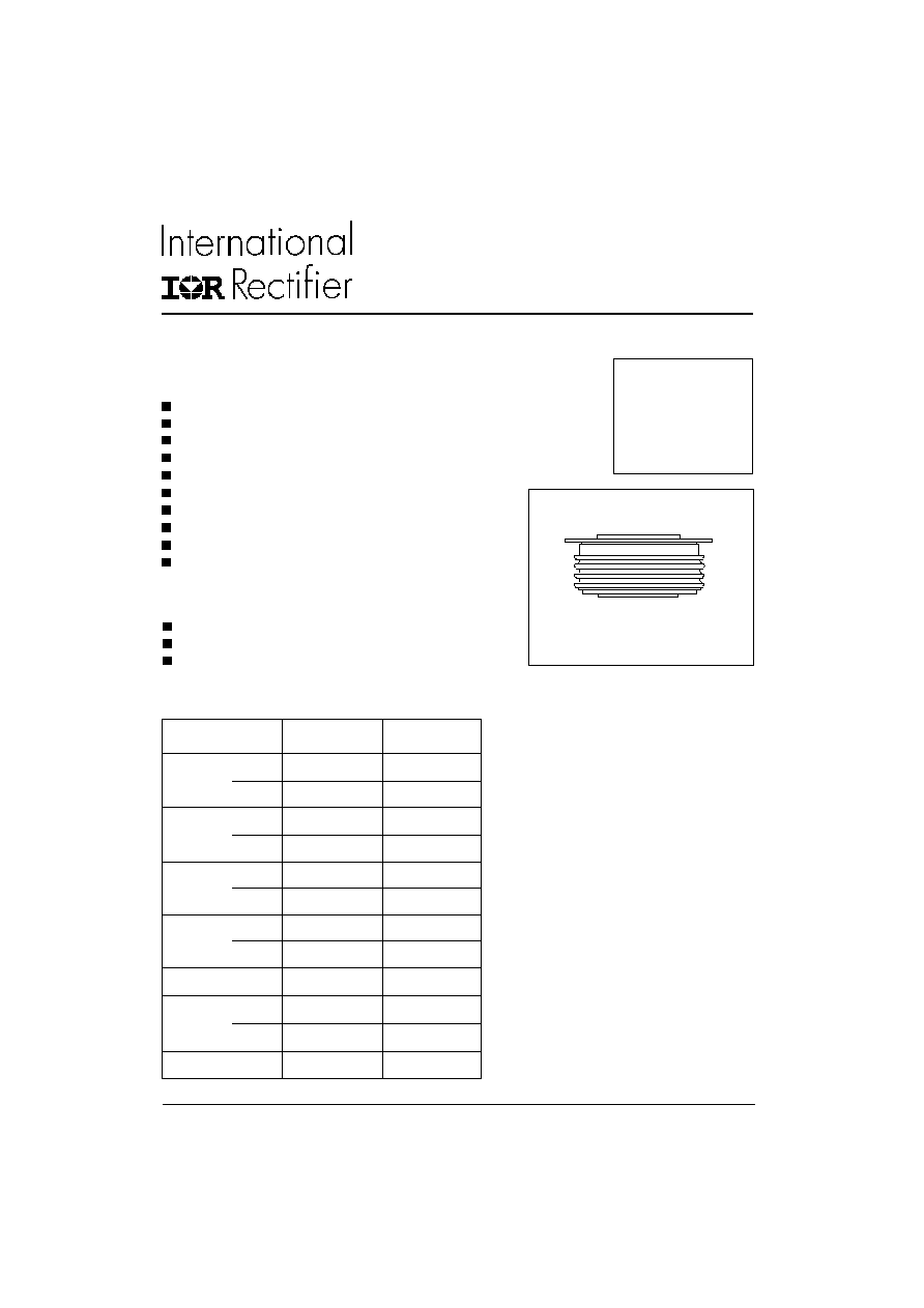
SD553C..S50L SERIES
FAST RECOVERY DIODES
Hockey Puk Version
560A
Bulletin I2092 rev. C 04/00
www.irf.com
Features
High power FAST recovery diode series
6.0 µs recovery time
High voltage ratings up to 4500V
High current capability
Optimized turn on and turn off characteristics
Low forward recovery
Fast and soft reverse recovery
Press-puk encapsulation
Case style conform to JEDEC DO-200AB (B-PUK)
Maximum junction temperature 125∞C
Typical Applications
Snubber diode for GTO
High voltage free-wheeling diode
Fast recovery rectifier applications
Major Ratings and Characteristics
I
F(AV)
560
A
@ T
hs
55
∞C
I
F(RMS)
1120
A
@ T
hs
25
∞C
I
FSM
@
50Hz
12000
A
@ 60Hz
12570
A
I
2
t
@
50Hz
721
KA
2
s
@ 60Hz
658
KA
2
s
V
RRM
range
3000 to 4500
V
t
rr
6.0
µs
@ T
J
125
∞C
T
J
- 40 to 125
∞C
Parameters
SD553C..S50L
Units
case style DO-200AB (B-PUK)

SD553C..S50L Series
2
Bulletin I2092 rev. C 04/00
www.irf.com
Voltage
V
RRM
, maximum repetitive
V
RSM
, maximum non-
I
RRM
max.
Type number
Code
peak reverse voltage
repetitive peak rev. voltage
@ T
J
= 125∞C
V
V
mA
30
3000
3100
36
3600
3700
40
4000
4100
45
4500
4600
ELECTRICAL SPECIFICATIONS
Voltage Ratings
SD553C..S50L
75
Test conditions
Max. values @ T
J
= 125
∞C
Code
(
µs)
(A)
(A/
µs)
(V)
(
µs)
(
µC)
(A)
Recovery Characteristics
S50
5.0
1000
100
- 50
6.0
900
250
Typical t
rr
I
pk
di/dt
V
r
t
rr
Q
rr
I
rr
@ 25% I
RRM
Square Pulse
@ 25% I
RRM
T
J
= 25
o
C
I
F(AV)
Max. average forward current
560 (210)
A
180∞ conduction, half sine wave
@ Heatsink temperature
55 (85)
∞C
Double side (single side) cooled
I
F(RMS)
Max. RMS forward current
1120
A
@ 25∞C heatsink temperature double side cooled
I
FSM
Max. peak, one-cycle forward,
12000
t = 10ms
No voltage
non-repetitive surge current
12570
t = 8.3ms
reapplied
10100
t = 10ms
50% V
RRM
10570
t = 8.3ms
reapplied
Sinusoidal half wave,
I
2
t
Maximum I
2
t for fusing
721
t = 10ms
No voltage
Initial T
J
= T
J
max.
658
t = 8.3ms
reapplied
510
t = 10ms
50% V
RRM
466
t = 8.3ms
reapplied
I
2
t
Maximum I
2
t for fusing
7210
KA
2
s t = 0.1 to 10ms, no voltage reapplied
V
F(TO)1
Low level value of threshold
voltage
V
F(TO)2
High level value of threshold
voltage
r
f
1
Low level value of forward
slope resistance
r
f
2
High level value of forward
slope resistance
V
FM
Max. forward voltage drop
3.24
V
I
pk
= 1500A, T
J
= 125∞C, t
p
= 10ms sinusoidal wave
Parameter
SD553C..S50L
Units
Conditions
Forward Conduction
KA
2
s
A
V
m
0.89
(I >
x I
F(AV)
),T
J
= T
J
max.
0.98
(16.7% x
x I
F(AV)
< I <
x I
F(AV)
), T
J
= T
J
max.
1.95
(I >
x I
F(AV)
),T
J
= T
J
max.
1.77
(16.7% x
x I
F(AV)
< I <
x I
F(AV)
), T
J
= T
J
max.
SD553C..S50L Series
3
Bulletin I2092 rev. C 04/00
www.irf.com
T
J
Max. junction operating temperature range
-40 to 125
T
stg
Max. storage temperature range
-40 to 150
R
thJ-hs
Max. thermal resistance,
0.073
DC operation single side cooled
junction to heatsink
0.031
DC operation double side cooled
F
Mounting force, ± 10%
14700
N
(1500)
(Kg)
wt
Approximate weight
255
g
Case style
DO-200AB (B-PUK)
Conforms to JEDEC
Parameter
SD553C..S50L
Units
Conditions
Thermal and Mechanical Specifications
∞C
K/W
180∞
0.009
0.009
0.006
0.006
T
J
= T
J
max.
120∞
0.011
0.011
0.011
0.011
90∞
0.014
0.014
0.015
0.015
K/W
60∞
0.020
0.020
0.021
0.021
30∞
0.036
0.036
0.036
0.036
Conduction angle
Units
Conditions
Single Side Double Side
Single Side Double Side
Sinusoidal conduction
Rectangular conduction
R
thJ-hs
Conduction
(The following table shows the increment of thermal resistence R
thJ-hs
when devices operate at different conduction angles than DC)
1
-
Diode
2
-
Essential part number
3
-
3 = Fast recovery
4
-
C = Ceramic Puk
5
-
Voltage code: Code x 100 = V
RRM
(See Voltage Ratings table)
6
-
t
rr
code
7
-
L = Puk Case DO-200AB (B-PUK)
SD
55
3
C
45 S50
L
1
2
3
4
5
6
7
Device Code
Ordering Information Table

SD553C..S50L Series
4
Bulletin I2092 rev. C 04/00
www.irf.com
Outline Table
Fig. 1 - Current Ratings Characteristics
Fig. 2 - Current Ratings Characteristics
BOTH ENDS
0.8 (0.03)
TWO PLACES
3.5(0.14) DIA. NOM. x
1.8(0.07) DEEP MIN.
34 (1.34) DIA. MAX.
5
8
.5
(
2
.3
0
)
D
I
A
.
M
A
X
.
26
.
9
(
1
.
06)
2
5
.4
(
1
)
BOTH ENDS
53 (2.09) DIA. MAX.
Conforms to JEDEC DO-200AB (B-PUK)
All dimensions in millimeters (inches)
1 0
2 0
3 0
4 0
5 0
6 0
7 0
8 0
9 0
1 0 0
1 1 0
1 2 0
1 3 0
0
1 0 0
2 0 0
3 0 0
4 0 0
5 0 0
6 0 0
3 0 ∞
6 0 ∞
9 0 ∞
1 8 0 ∞
D C
1 2 0 ∞
A v e ra g e F o rw a r d C u rre n t ( A )
M
a
xi
m
u
m
A
l
l
o
w
a
bl
e
He
at
s
i
n
k
T
e
m
p
e
r
at
u
r
e
(
∞
C
)
C o nd uc tio n Pe riod
SD 5 5 3 C ..S 5 0 L S e rie s
( Sin g le S id e C o o le d )
R ( D C ) = 0 .0 7 3 K/ W
thJ -hs
3 0
4 0
5 0
6 0
7 0
8 0
9 0
1 0 0
1 1 0
1 2 0
1 3 0
0
1 0 0
2 0 0
3 0 0
4 0 0
3 0 ∞
6 0 ∞
9 0 ∞
1 2 0 ∞
1 8 0 ∞
A v e ra g e F o r w a rd C u rr e n t ( A )
M
a
xi
m
u
m
A
l
l
o
w
a
bl
e
He
at
s
i
n
k
T
e
m
p
e
r
at
u
r
e
(
∞
C)
Co nd uc tio n A ng le
S D 5 5 3 C ..S5 0 L S e rie s
( S in g le Sid e C o o le d )
R ( D C ) = 0 .0 7 3 K / W
th J- hs
Quote between upper and lower
pole pieces has to be considered
after application of Mounting Force
(see Thermal and Mechanical
Specification)

SD553C..S50L Series
5
Bulletin I2092 rev. C 04/00
www.irf.com
Fig. 3 - Current Ratings Characteristics
Fig. 4 - Current Ratings Characteristics
Fig. 5 - Forward Power Loss Characteristics
Fig. 6 - Forward Power Loss Characteristics
Fig. 7 - Maximum Non-repetitive Surge Current
Single and Double Side Cooled
Fig. 8 - Maximum Non-repetitive Surge Current
Single and Double Side Cooled
2 0
3 0
4 0
5 0
6 0
7 0
8 0
9 0
1 0 0
1 1 0
1 2 0
1 3 0
0
1 0 0 2 0 0 3 0 0 4 0 0 5 0 0 6 0 0 7 0 0 8 0 0
3 0 ∞
6 0 ∞
9 0 ∞
1 2 0 ∞
1 8 0 ∞
A v e ra g e Fo rw a r d C u rre n t ( A )
M
a
x
i
mu
m A
l
l
o
w
a
b
l
e
H
e
a
t
s
i
n
k
T
e
mp
e
r
a
t
u
r
e
(
∞
C)
C o nd uc tio n Ang le
S D 5 5 3 C ..S 5 0 L Se rie s
( D o u b le Sid e C o o le d )
R ( D C ) = 0 .0 3 1 K / W
t hJ -hs
1 0
2 0
3 0
4 0
5 0
6 0
7 0
8 0
9 0
10 0
11 0
12 0
13 0
0
2 00
40 0
6 00
80 0
1 00 0
1 20 0
30 ∞
60 ∞
90∞
18 0∞
D C
120∞
Aver age Forw ard Curr en t (A)
M
a
x
i
mu
m
A
l
l
o
w
a
bl
e
He
at
s
i
n
k
T
e
m
p
e
r
at
u
r
e
(
∞
C)
C o nd uc tio n Pe rio d
SD 553 C..S50 L Series
(Double Side Cooled)
R (DC) = 0.031 K/W
thJ -h s
0
2 50
5 00
7 50
10 0 0
12 5 0
15 0 0
17 5 0
20 0 0
22 5 0
25 0 0
0
1 00 2 0 0 3 0 0 4 0 0 5 00 60 0 70 0 8 0 0
1 80∞
1 20∞
90∞
60∞
30∞
Averag e Forw ard Current (A)
Ma
x
i
m
u
m
A
v
e
r
a
g
e
F
o
r
w
a
r
d
P
o
w
e
r
L
o
s
s
(
W
)
RMS Lim it
Co n d uc tio n An g le
SD5 53C..S50L Series
T = 125 ∞C
J
0
5 00
1 0 00
1 5 00
2 0 00
2 5 00
3 0 00
3 5 00
0
2 00
4 0 0
6 00
8 0 0
10 0 0
12 0 0
DC
180∞
120∞
90∞
60∞
30∞
Average Forwar d Current (A)
RM S Lim it
M
a
x
i
m
u
m
A
v
e
r
a
g
e
F
o
rw
a
r
d
P
o
w
e
r L
o
s
s
(
W
)
C o nd uc tio n Pe rio d
SD553 C..S50L Series
T = 125∞C
J
3 0 0 0
4 0 0 0
5 0 0 0
6 0 0 0
7 0 0 0
8 0 0 0
9 0 0 0
1 0 0 0 0
1 1 0 0 0
1 2 0 0 0
1
1 0
1 0 0
N um b e r O f E q ua l A m p litud e H a lf Cy c le C urre n t Pulse s (N )
P
e
ak
Hal
f
S
i
n
e
W
a
v
e
Fo
r
w
ar
d C
u
r
r
e
n
t
(
A
)
S D 5 5 3 C ..S5 0 L S e rie s
In it ia l T = 1 2 5 ∞C
@ 6 0 H z 0 .0 0 8 3 s
@ 5 0 H z 0 .0 1 0 0 s
A t A n y R a te d L o a d C o n d it io n A n d W it h
5 0 % R a t e d V A p p lie d Fo llo w in g S u rg e
R RM
J
2 0 0 0
4 0 0 0
6 0 0 0
8 0 0 0
1 0 0 0 0
1 2 0 0 0
1 4 0 0 0
0 .0 1
0 .1
1
P u lse T ra in D u ra tio n ( s)
M ax im u m N o n R e pe t it iv e Su rg e C u rre nt
P
e
ak
Hal
f
S
i
n
e
W
a
v
e
Fo
r
w
ar
d C
u
r
r
e
n
t
(
A
)
S D 5 5 3 C ..S 5 0 L S e rie s
In itial T = 1 2 5∞C
N o V o lta g e Re ap plie d
5 0 % R at e d V R e ap p lie d
V e rsu s P ulse T ra in D u rat io n .
R RM
J

SD553C..S50L Series
6
Bulletin I2092 rev. C 04/00
www.irf.com
Fig. 10 - Thermal Impedance Z
thJ-hs
Characteristic
Fig. 9 - Forward Voltage Drop Characteristics
Fig. 11 - Typical Forward Recovery Characteristics
Fig. 12 - Recovery Time Characteristics
Fig. 13 - Recovery Charge Characteristics
Fig. 14 - Recovery Current Characteristics
1 00
1 00 0
1 0 00 0
1 .5
2
2. 5
3
3.5
4
4 .5
5
T = 25 ∞C
J
In stan tan eous Forward V oltage (V )
I
n
st
a
n
t
a
n
e
o
u
s
F
o
r
w
a
r
d
C
u
rr
e
n
t
(
A
)
T = 125∞C
J
SD55 3C..S5 0L Series
0 . 0 0 1
0 . 0 1
0 . 1
0 . 0 0 1
0 . 0 1
0 . 1
1
1 0
1 0 0
Sq u a re W a v e P u lse D u ra t io n ( s)
th
J
-
h
s
T
r
a
n
s
i
e
n
t
T
h
e
r
m
a
l
I
m
p
e
d
a
n
c
e
Z
(
K
/
W
)
St e a d y S ta t e V a lu e
R = 0 . 0 7 3 K / W
( Sin g le S id e C o o le d )
R = 0 . 0 3 1 K / W
( D o ub le S id e C o o le d )
( D C O p e ra t io n )
t hJ -hs
thJ - hs
SD 5 5 3 C . . S5 0 L S e rie s
0
5 0
1 0 0
1 5 0
2 0 0
2 5 0
3 0 0
3 5 0
4 0 0
0
2 0 0
4 0 0
6 0 0
8 0 0
1 0 0 0
1 2 0 0
1 4 0 0
1 6 0 0
1 8 0 0
2 0 0 0
Fo
r
w
ar
d R
e
c
o
v
e
r
y
(
V
)
T = 1 2 5 ∞C
T = 2 5 ∞C
J
J
SD 5 5 3 C . .S 5 0 L S e rie s
R at e O f R ise O f Fo rw a rd C u rre n t - d i/d t ( A / us)
I
V
F P
0
1 0 0
2 0 0
3 0 0
4 0 0
5 0 0
6 0 0
7 0 0
8 0 0
0
5 0
1 0 0 1 5 0 2 0 0 2 5 0 3 0 0
I = 1 5 00 A
Sin e Puls e
FM
1 00 0 A
50 0 A
R a te O f F a ll O f F o rwa rd Current - d i/d t (A /µs )
M
a
x
i
m
u
m
Re
v
e
r
s
e
Re
c
o
v
e
r
y
C
u
r
r
e
n
t
-
I
r
r
(
A
)
SD 5 5 3 C ..S5 0 L S e r ie s
T = 1 2 5 ∞C ; V > 1 0 0 V
J
r
0
5 0 0
1 0 0 0
1 5 0 0
2 0 0 0
2 5 0 0
0
5 0
1 0 0 1 5 0 2 0 0 2 5 0 3 0 0
Ra te O f F a ll O f F o rwa rd C urre nt - d i/d t ( A/µs )
SD 5 5 3 C ..S5 0 L S e rie s
T = 1 2 5 ∞C ; V > 1 0 0 V
I = 15 00 A
Sine Pulse
F M
1 00 0 A
5 0 0 A
J
r
M
a
x
i
m
u
m
R
e
v
e
rs
e
R
e
c
o
v
e
ry
C
h
a
r
g
e
-
Q
rr (
µ
C
)
4
4 . 5
5
5 . 5
6
6 . 5
7
7 . 5
8
8 . 5
9
9 . 5
1 0
1 0 .5
1 0
1 0 0
1 0 0 0
Ra te O f Fa ll O f F orw a rd Current - d i/d t ( A/µs )
M
a
x
i
m
u
m
R
e
v
e
rs
e
R
e
c
o
v
e
ry
T
i
m
e
-
T
rr
(
µ
s
)
50 0 A
I = 15 00 A
Sin e Pu ls e
100 0 A
SD 5 5 3 C ..S5 0 L Se rie s
T = 1 2 5 ∞ C ; V > 1 0 0 V
J
FM
r

SD553C..S50L Series
7
Bulletin I2092 rev. C 04/00
www.irf.com
Fig. 18 - Frequency Characteristics
Fig. 17 - Maximum Total Energy Loss Per Pulse Characteristics
Fig. 20 - Frequency Characteristics
Fig. 19 - Maximum Total Energy Loss Per Pulse Characteristics
Fig. 15 - Maximum Total Energy Loss Per Pulse Characteristics
Fig. 16 - Frequency Characteristics
1 E2
1 E3
1 E4
1 E1
1E2
1E 3
1E 4
1
2
Pulse Basewidth (µs)
Pe
a
k
F
o
r
w
a
r
d
C
u
r
r
e
n
t (
A
)
1 0 jo ule s p e r p uls e
6
4
Si nu so id al Pu lse
SD 5 5 3 C ..S5 0 L S eri es
0 .8
0 .6
0. 4
0 .2
T = 1 25 ∞ C , V = 1 5 0 0 V
J
R R M
d v /d t = 1 0 0 0 V/ µ s
tp
1E 2
1E 3
1E 4
1 E1
1E 2
1 E3
1E 4
Pulse Bas ew idth (µs)
50 H z
2 0 0
10 0 0 0
1 00
4 00 0
d v / dt = 1 0 0 0 V/ u s
4 0 0
1 0 0 0
2 0 0 0
6 0 0 0
P
e
a
k
F
o
rw
a
r
d
C
u
rre
n
t
(
A
)
Si nu so id al Pu ls e
S D 55 3 C..S5 0 L Se rie s
3 0 0 0
1 50 0
T = 5 5 ∞C , V = 1 5 0 0 V
C
RR M
tp
6 00
1 E2
1 E3
1 E4
1 E1
1E 2
1E 3
1E 4
1
2
Pulse Basewidth (µs)
P
e
a
k
F
o
r
w
a
r
d
C
u
rre
n
t
(
A
)
10 jo ules p e r p uls e
6
4
d v/ d t = 1 0 0 0 V/ µ s
T = 1 25 ∞C , V = 15 0 0 V
J
R RM
Sin uso id al Pu ls e
0.8
0 .6
0.4
8
SD 5 5 3 C.. S5 0 L Se rie s
tp
1E2
1E3
1E4
1E 1
1E 2
1E 3
1 E4
Pu lse Basew idth (µs)
Trap e zo idal Pul se
50 H z
1 00
2 0 0
4 0 0
10 0 0
1 50 0
2 0 00
40 0 0
3 0 0 0
6 0 0
T = 5 5 ∞C, V = 1 5 0 0 V
R R M
6 00 0
P
e
ak
F
o
r
w
ar
d C
u
r
r
e
n
t
(
A
)
SD 55 3C ..S5 0 L S er ie s
dv / dt = 10 0 0 V/u s,
di/ d t = 3 0 0 A / us
C
tp
1 E 2
1 E 3
1 E 4
1E1
1E2
1E3
1 E4
1
2
Pulse Basew idth (µs)
4
10 jo u le s p e r p uls e
6
Tra pez o idal Pul se
P
e
ak
F
o
r
w
ar
d C
u
r
r
e
n
t
(
A
)
T = 1 2 5 ∞C , V = 1 5 0 0 V
J
R R M
dv / d t = 1 00 0V / µs
di /d t = 1 0 0 A / µs
0 .8
0.6
SD 5 5 3 C..S5 0 L Se rie s
tp
8
0 .4
1 E2
1 E3
1 E4
1 E1
1 E2
1 E3
1 E4
Pulse Bas ew idth (µs)
Tra pe zo ida l Pu lse
50 H z
10 0
20 0
4 00
1 0 0 0
15 0 0
2 00 0
4 0 0 0
3 00 0
60 0
T = 5 5 ∞ C, V = 1 5 00 V
R R M
6 0 0 0
P
e
ak
F
o
r
w
ar
d C
u
r
r
e
n
t
(
A
)
SD 5 5 3 C ..S 50 L Se ri e s
d v /d t = 1 0 0 0 V /u s,
d i/ dt = 1 0 0 A /u s
C
tp