Features
Center amplifying gate
Hermetic metal case with ceramic insulator
International standard case TO-209AE (TO-118)
Compression Bonded Encapsulation for heavy duty
operations such as severe thermal cycling
Typical Applications
DC motor controls
Controlled DC power supplies
AC controllers
case style
TO-209AE (TO-118)
330A
PHASE CONTROL THYRISTORS
Stud Version
ST330S SERIES
1
Bulletin I25156 rev. C 03/03
www.irf.com
I
T(AV)
330
A
@ T
C
75
įC
I
T(RMS)
520
A
I
TSM
@
50Hz
9000
A
@ 60Hz
9420
A
I
2
t
@
50Hz
405
KA
2
s
@ 60Hz
370
KA
2
s
V
DRM
/V
RRM
400 to 2000
V
t
q
typical
100
Ķs
T
J
- 40 to 125
įC
Parameters
ST330S
Units
Major Ratings and Characteristics
ST330S Series
2
www.irf.com
Bulletin I25156 rev. C 03/03
ELECTRICAL SPECIFICATIONS
Voltage Ratings
Voltage
V
DRM
/V
RRM
, max. repetitive
V
RSM
, maximum non-
I
DRM
/I
RRM
max.
Type number
Code
peak and off-state voltage
repetitive peak voltage
@ T
J
= T
J
max
V
V
mA
04
400
500
08
800
900
ST330S
12
1200
1300
50
16
1600
1700
20
2000
2100
On-state Conduction
I
T(AV)
Max. average on-state current
330
A
180į conduction, half sine wave
@ Case temperature
75
įC
I
T(RMS)
Max. RMS on-state current
520
A
DC @ 75įC case temperature
I
TSM
Max. peak, one-cycle
9000
t = 10ms
No voltage
non-repetitive surge current
9420
t = 8.3ms
reapplied
7570
t = 10ms
100% V
RRM
7920
t = 8.3ms
reapplied
Sinusoidal half wave,
I
2
t
Maximum I
2
t for fusing
405
t = 10ms
No voltage
Initial T
J
= T
J
max.
370
t = 8.3ms
reapplied
287
t = 10ms
100% V
RRM
262
t = 8.3ms
reapplied
I
2
t
Maximum I
2
t for fusing
4050
KA
2
s
t = 0.1 to 10ms, no voltage reapplied
V
T(TO)1
Low level value of threshold
voltage
V
T(TO)2
High level value of threshold
voltage
r
t
1
Low level value of on-state
slope resistance
r
t
2
High level value of on-state
slope resistance
V
TM
Max. on-state voltage
1.52
V
I
pk
= 1000A, T
J
= T
J
max, t
p
= 10ms sine pulse
I
H
Maximum holding current
600
I
L
Max. (typical) latching current
1000
0.834
(16.7% x
x I
T(AV)
< I <
x I
T(AV)
), T
J
= T
J
max.
0.687
(16.7% x
x I
T(AV)
< I <
x I
T(AV)
), T
J
= T
J
max.
0.636
(I >
x I
T(AV)
),T
J
= T
J
max.
Parameter
ST330S
Units Conditions
0.898
(I >
x I
T(AV)
),T
J
= T
J
max.
KA
2
s
V
m
mA
T
J
= 25įC, anode supply 12V resistive load
A
ST330S Series
www.irf.com
3
Bulletin I25156 rev. C 03/03
Parameter
ST330S
Units Conditions
Switching
t
q
Typical turn-off time
100
t
d
Typical delay time
1.0
di/dt
Max. non-repetitive rate of rise
Gate drive 20V, 20
, t
r
1Ķs
of turned-on current
T
J
= T
J
max, anode voltage
80% V
DRM
Gate current A, di
g
/dt = 1A/Ķs
V
d
= 0.67% V
DRM
,
T
J
= 25įC
I
TM
= 550A, T
J
= T
J
max, di/dt
= 40A/Ķs, V
R
= 50V
dv/dt
= 20V/Ķs, Gate 0V 100
,
t
p
= 500Ķs
1000
A/Ķs
Ķs
dv/dt
Maximum critical rate of rise of
off-state voltage
I
RRM
Max. peak reverse and off-state
I
DRM
leakage current
Blocking
500
V/Ķs
T
J
= T
J
max. linear to 80% rated V
DRM
Parameter
ST330S
Units Conditions
50
mA
T
J
= T
J
max, rated V
DRM
/V
RRM
applied
P
GM
Maximum peak gate power
10.0
T
J
= T
J
max, t
p
5ms
P
G(AV)
Maximum average gate power
2.0
T
J
= T
J
max, f = 50Hz, d% = 50
I
GM
Max. peak positive gate current
3.0
A
T
J
= T
J
max, t
p
5ms
+V
GM
Maximum peak positive
gate voltage
-V
GM
Maximum peak negative
gate voltage
I
GT
DC gate current required
T
J
= - 40įC
to trigger
mA
T
J
= 25įC
T
J
= 125įC
V
GT
DC gate voltage required
T
J
= - 40įC
to trigger
V
T
J
= 25įC
T
J
= 125įC
I
GD
DC gate current not to trigger
10
mA
Parameter
ST330S
Units Conditions
20
5.0
Triggering
V
GD
DC gate voltage not to trigger
0.25
V
T
J
= T
J
max
TYP.
MAX.
200
-
100
200
50
-
2.5
-
1.8
3.0
1.1
-
Max. gate current/ voltage not to
trigger is the max. value which
will not trigger any unit with rated
V
DRM
anode-to-cathode applied
Max. required gate trigger/ cur-
rent/ voltage are the lowest value
which will trigger all units 12V
anode-to-cathode applied
W
V
T
J
= T
J
max, t
p
5ms
ST330S Series
4
www.irf.com
Bulletin I25156 rev. C 03/03
Ordering Information Table
1
-
Thyristor
2
-
Essential part number
3
-
0 = Converter grade
4
-
S = Compression bonding Stud
5
-
Voltage code: Code x 100 = V
RRM
(See Voltage Rating Table)
6
-
P = Stud base 3/4"-16UNF-2A threads
7
-
0 = Eyelet terminals (Gate and Auxiliary Cathode Leads)
1 = Fast - on terminals (Gate and Auxiliary Cathode Leads)
Device Code
5
1
2
3
4
ST
33
0
S
16
P
0
7
6
T
J
Max. operating temperature range
-40 to 125
T
stg
Max. storage temperature range
-40 to 150
R
thJC
Max. thermal resistance,
junction to case
R
thCS
Max. thermal resistance,
case to heatsink
T
Mounting torque, Ī 10%
48.5
(425)
wt
Approximate weight
535
g
Case style
TO - 209AE (TO-118)
See Outline Table
Parameter
ST330S
Units Conditions
0.10
DC operation
0.03
Mounting surface, smooth, flat and greased
Thermal and Mechanical Specification
įC
K/W
Non lubricated threads
Nm
(lbf-in)
R
thJC
Conduction
(The following table shows the increment of thermal resistence R
thJC
when devices operate at different conduction angles than DC)
180į
0.011
0.008
120į
0.013
0.014
90į
0.017
0.018
K/W
T
J
= T
J
max.
60į
0.025
0.026
30į
0.041
0.041
Conduction angle Sinusoidal conduction Rectangular conduction Units
Conditions
ST330S Series
www.irf.com
5
Bulletin I25156 rev. C 03/03
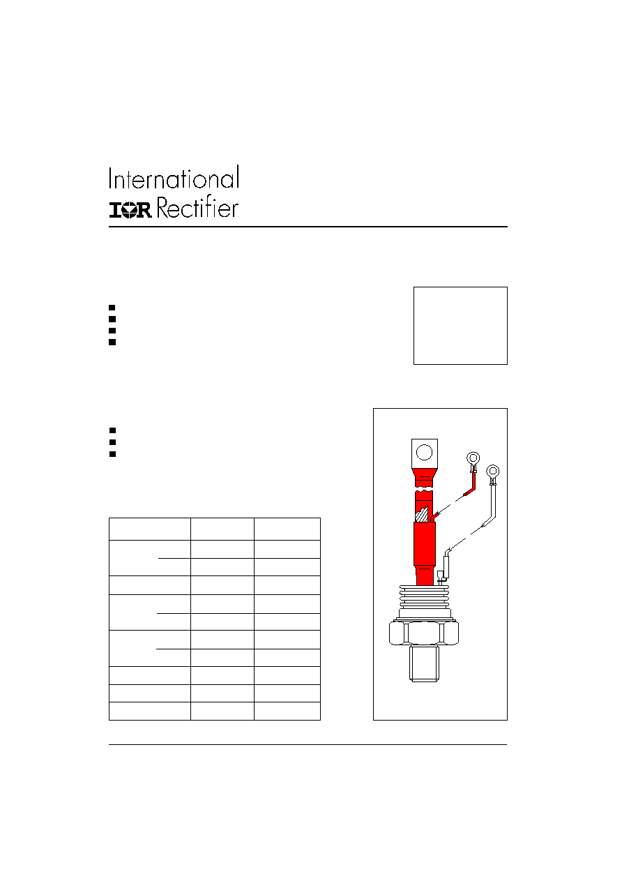
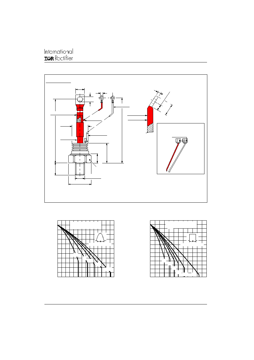
Fast-on Terminals
Case Style TO-209AE (TO-118)
All dimensions in millimeters (inches)
Outline Table
RED CATHODE
RED SILICON RUBBER
10.5 (0.41)
24
5 (
9
.
6
5
)
Ī
1
0
(
0
.
3
9)
WHITE GATE
4.3 (0.17) DIA.
CERAMIC HOUSING
WHITE SHRINK
NOM.
47
(
1
.
8
5)
M
AX.
24
5
(
9
.
6
5
)
38 (1.50)
MAX. DIA.
22 (0.87) MAX.
MA
X.
21
(
0
.
8
2
)
M
A
X
.
SW 45
2
FLEXIBLE LEAD
4.5 (0.18) MAX.
C.S. 50mm
(0.078 s.i.)
25
5 (
1
0.
0
4
)
RED SHRINK
22
(0
.8
6)
M
IN
.
49 (1.92) MAX.
3/4"16 UNF-2A
27
.
5
(
1
.
0
8
)
9.
5
(0
.3
7)
M
IN
.
AMP. 280000-1
REF-250
* FOR METRIC DEVICE: M24 X 1.5 - LENGHT 21 (0.83) MAX.
CONTACT FACTORY
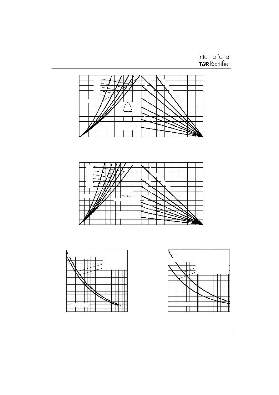
Fig. 1 - Current Ratings Characteristics
Fig. 2 - Current Ratings Characteristics
70
80
90
100
110
120
130
0
50
100 150 200 250 300 350
M
a
x
i
mu
m A
l
l
o
w
a
b
l
e
Ca
s
e
T
e
mp
er
a
t
u
r
e
(į
C)
30į
60į
90į
120į
180į
Average On-state Current (A)
Conduc tion Angle
ST330S Series
R (DC) = 0.10 K/ W
thJC
60
70
80
90
100
110
120
130
0
100
200
300
400
500
600
DC
30į
60į
90į
120į
180į
Average On-state Current (A)
M
a
x
i
m
u
m A
l
l
o
w
a
b
l
e
Ca
s
e
T
e
m
p
er
at
u
r
e
(
į
C
)
Conduction Period
ST330S Series
R (DC) = 0.10 K/ W
thJC
ST330S Series
6
www.irf.com
Bulletin I25156 rev. C 03/03
Fig. 5 - Maximum Non-Repetitive Surge Current
Fig. 6 - Maximum Non-Repetitive Surge Current
3500
4000
4500
5000
5500
6000
6500
7000
7500
8000
1
10
100
Number Of Equal Amplitude Half Cycle Current Pulses (N)
Pe
a
k
H
a
l
f
S
i
n
e
W
a
v
e
O
n
-s
t
a
t
e
C
u
rre
n
t
(
A
)
Initial T = 125įC
@ 60 Hz 0.0083 s
@ 50 Hz 0.0100 s
J
ST330S Series
At Any Rated Load Condition And With
Rated V Applied Following Surge.
RRM
3000
4000
5000
6000
7000
8000
9000
0.01
0.1
1
Pulse Train Duration (s)
Versus Pulse Train Duration. Control
P
e
a
k
H
a
l
f
S
i
n
e
W
a
v
e
O
n
-
s
t
a
t
e
C
u
r
r
e
n
t
(
A
)
Initial T = 125įC
No Voltage Reapplied
Rated V Reapplied
RRM
J
ST330S Series
Maximum Non Repetitive Surge Current
Of Conduction May Not Be Maintained.
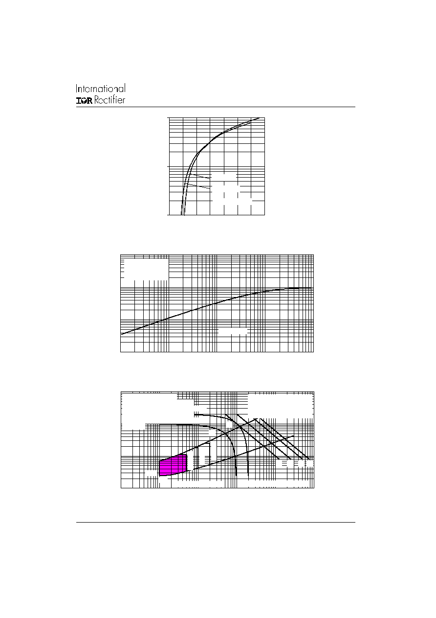
Fig. 3 - On-state Power Loss Characteristics
Fig. 4 - On-state Power Loss Characteristics
25
50
75
100
125
Maximum Allowable Ambient Temperature (įC)
0.0
8 K
/ W
0.2 K
/ W
0.3 K
/ W
0.4 K/
W
0.6 K/W
1.2 K/ W
R
=
0.
03
K
/W
- D
elt
a R
th
SA
0.1
2 K
/ W
0
40
80
120
160
200
240
280
320
360
400
440
480
0
50
100 150 200 250 300 350
180į
120į
90į
60į
30į
RMS Limit
Conduction Angle
M
a
x
i
m
u
m
A
v
er
a
g
e O
n
-
s
ta
t
e
P
o
we
r
L
o
s
s
(
W
)
Average On-state Current (A)
ST330S Series
T = 125įC
J
25
50
75
100
125
Maximum Allowable Ambient Temperature (įC)
R
=
0
.0
3
K/
W
- D
elta
R
th
SA
0.0
8 K
/W
0.1
2 K
/ W
0.2 K
/ W
0.3 K/W
0.4 K/ W
0.6 K/W
1.2 K/W
0
50
100
150
200
250
300
350
400
450
500
550
600
650
0
100
200
300
400
500
600
DC
180į
120į
90į
60į
30į
RMS Limit
Conduction Period
M
a
x
i
mu
m A
v
e
r
ag
e
O
n
-
s
t
a
t
e
P
o
wer
L
o
s
s
(
W
)
Average On-state Current (A)
ST330S Series
T = 125įC
J
ST330S Series
www.irf.com
7
Bulletin I25156 rev. C 03/03
Fig. 8 - Thermal Impedance Z
thJC
Characteristic
0.001
0.01
0.1
1
0.001
0.01
0.1
1
10
Square Wave Pulse Duration (s)
th
J
C
ST330S Series
Steady State Value
R = 0.10 K/ W
(DC Operation)
thJC
T
r
a
n
s
i
e
n
t
T
h
e
r
m
a
l
I
m
p
e
d
a
n
c
e
Z
(
K
/
W
)
Fig. 9 - Gate Characteristics
0.1
1
10
100
0.001
0.01
0.1
1
10
100
VGD
IGD
(b)
(a)
Tj
=
2
5
į
C
Tj
=
1
2
5
į
C
T
j
=
-
40 į
C
(2) (3)
Instantaneous Gate Current (A)
I
n
s
t
a
n
t
a
ne
ou
s
G
a
t
e
V
o
l
t
a
g
e
(
V
)
Rectangular gate pulse
a) Recommended load line for
b) Recommended load line for
<=30% rated di/ dt : 10V, 10ohms
Frequency Limited by PG(AV)
rated di/ dt : 20V, 10ohms; tr<=1 Ķs
tr<=1 Ķs
(1)
(1) PGM = 10W, tp = 4ms
(2) PGM = 20W, tp = 2ms
(3) PGM = 40W, tp = 1ms
(4) PGM = 60W, tp = 0.66ms
Device: ST330S Series
(4)
Fig. 7 - On-state Voltage Drop Characteristics
Instantaneous On-state Voltage (V)
Instantaneous On-state Current (A)
100
1000
10000
0
1
2
3
4
5
6
7
Tj = 25įC
Tj = 125įC
ST330S Series
ST330S Series
8
www.irf.com
Bulletin I25156 rev. C 03/03
IR WORLD HEADQUARTERS: 233 Kansas St., El Segundo, California 90245, USA Tel: (310) 252-7105
TAC Fax: (310) 252-7309
Visit us at www.irf.com for sales contact information. 03/03
Data and specifications subject to change without notice.
This product has been designed and qualified for Industrial Level.
Qualification Standards can be found on IR's Web site.