Äîêóìåíòàöèÿ è îïèñàíèÿ www.docs.chipfind.ru
1
UFB120FA40
Bulletin PD-20488 12/01
V
R
Cathode-to-Anode Voltage
400
V
I
F
Continuous Forward Current, T
C
= 65°C
Per Diode
60
A
I
FSM
Single Pulse Forward Current, T
C
= 25°C
Per Diode
800
P
D
Max. Power Dissipation, T
C
@ 90°C
Per Module
96
W
V
ISOL
RMS Isolation Voltage, Any Terminal to Case, t = 1 min
2500
V
T
J
,
T
STG
Operating Junction and Storage Temperatures
- 55 to 150
°C
Parameters
Max
Units
Absolute Maximum Ratings
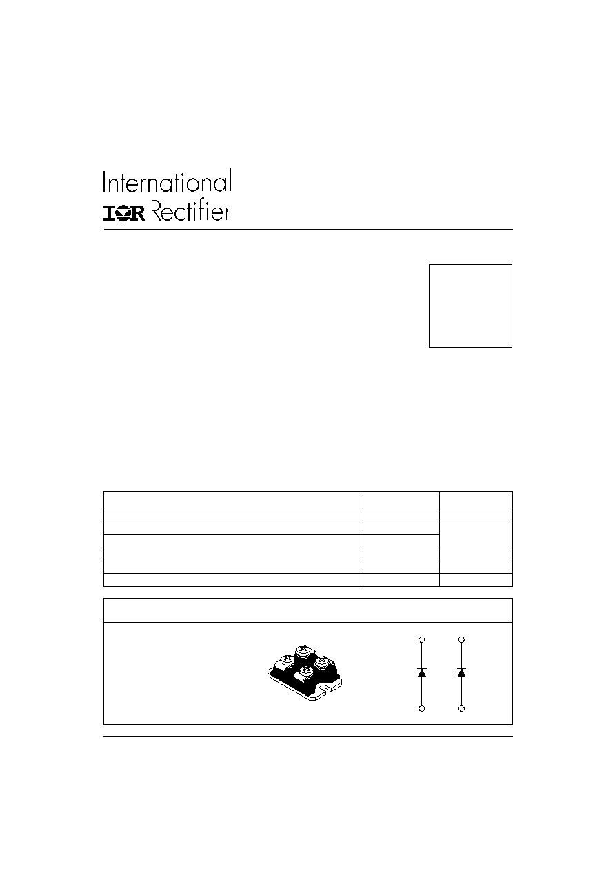
Case Styles
UFB120FA40
www.irf.com
2
1
4
3
SOT-227
Features
Description
t
rr
= 35ns
I
F(AV)
= 120A
@ T
C
= 65°C
V
R
= 400V
Insulated Ultrafast Rectifier Module
· Two Fully Independent Diodes
· Ceramic Fully Insulated Package (V
ISOL
= 2500V AC)
· Ultrafast Reverse Recovery
· Ultrasoft Reverse Recovery Current Shape
· Low Forward Voltage
· Optimized for Power Conversion: Welding and Industrial SMPS Applications
· Industry Standard Outline
· Plug-in Compatible with other SOT-227 Packages
· Easy to Assemble
· Direct Mounting to Heatsink
The UFB120FA40 insulated modules integrate two state-of-the-art International Rectifier's Ultrafast recovery rectifiers
in the compact, industry standard SOT-227 package. The planar structure of the diodes, and the platinum doping life-
time control, provide a Ultrasoft recovery current shape, together with the best overall performance, ruggedness and
reliability characteristics.
These devices are thus intended for high frequency applications in which the switching energy is designed not to be
predominant portion of the total energy, such as in the output rectification stage of Welding machines, SMPS, DC-
DC converters. Their extremely optimized stored charge and low recovery current reduce both over dissipation in the
switching elements (and snubbers) and EMI/ RFI.
UFB120FA40
Bulletin PD-20488 12/01
2
www.irf.com
V
BR
Cathode Anode
400
-
-
V
I
R
= 100µA
Breakdown Voltage
V
FM
Forward Voltage
-
1.16 1.37
V
I
F
= 60A
-
0.96 1.13
V
I
F
= 60A, T
J
= 150°C
I
RM
Reverse Leakage Current
-
-
0.1
mA
V
R
= V
R
Rated
-
-
1
mA
T
J
= 150°C, V
R
= V
R
Rated
C
T
Junction Capacitance
-
67
-
pF
V
R
= 400V
Electrical Characteristics @ T
J
= 25°C (unless otherwise specified) per diode
Parameters
Min Typ Max Units Test Conditions
R
thJC
Junction to Case
Single Diode Conducting
-
0.99
1.24
°C/W
Both Diodes Conducting
-
0.49
0.62
°C/W
R
thCS
Case to Heat Sink, Flat, Greased Surface
-
0.05
-
Wt
Weight
-
30
-
g
T
Mounting Torque
-
1.3
-
(N*m)
Parameters
Min
Typ
Max
Units
Thermal - Mechanical Characteristics
Dynamic Recovery Characteristics @ T
J
= 25°C (unless otherwise specified) per diode
t
rr
Reverse Recovery Time
-
30
35
ns
I
F
= 1.0A, di
F
/dt = 200A/µs, V
R
= 30V
-
65
-
T
J
= 25°C
-
128
-
T
J
= 125°C
I
RRM
Peak Recovery Current
-
7.4
-
A
T
J
= 25°C
-
17.8
-
T
J
= 125°C
Q
rr
Reverse Recovery Charge
-
240
-
nC
T
J
= 25°C
-
1139
-
T
J
= 125°C
I
F
= 50A
V
R
= 200V
di
F
/dt = 200A/µs
Parameters
Min Typ Max Units Test Conditions
Bulletin PD-20488 12/01
UFB120FA40
3
www.irf.com
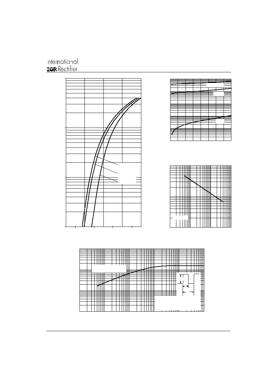
Fig. 2 - Typical Values Of Reverse Current
Vs. Reverse Voltage
Fig. 1 - Typical Forward Voltage Drop Characteristics
(per diode)
Fig. 3 - Typical Junction Capacitance
Vs. Reverse Voltage
Forward Voltage Drop - V
FM
(V)
Instantaneous Forward Current - I
F
(A)
Reverse Voltage - V
R
(V)
Reverse Voltage - V
R
(V)
Junction Capacitance - C
T
(pF)
Fig. 4 - Max. Thermal Impedance Z
thJC
(per diode)
t
1
, Rectangular Pulse Duration (Seconds)
Thermal Impedance Z
thJC
(°C/W)
Reverse Current - I
R
(µA)
1
10
100
1000
0
0.5
1
1.5
2
Tj = 150°C
Tj = 125°C
Tj = 25°C
0.001
0.01
0.1
1
10
100
0
100
200
300
400
125°C
25°C
Tj = 150°C
10
100
1000
1
10
100
1000
Tj = 25°C
0.01
0.1
1
10
0.0001
0.001
0.01
0.1
1
10
Single Pulse
(Thermal Impedance)
2
t
1
t
P
DM
Notes:
1. Duty factor D = t1/ t2
2. Peak Tj = Pdm x ZthJC + Tc
UFB120FA40
Bulletin PD-20488 12/01
4
www.irf.com
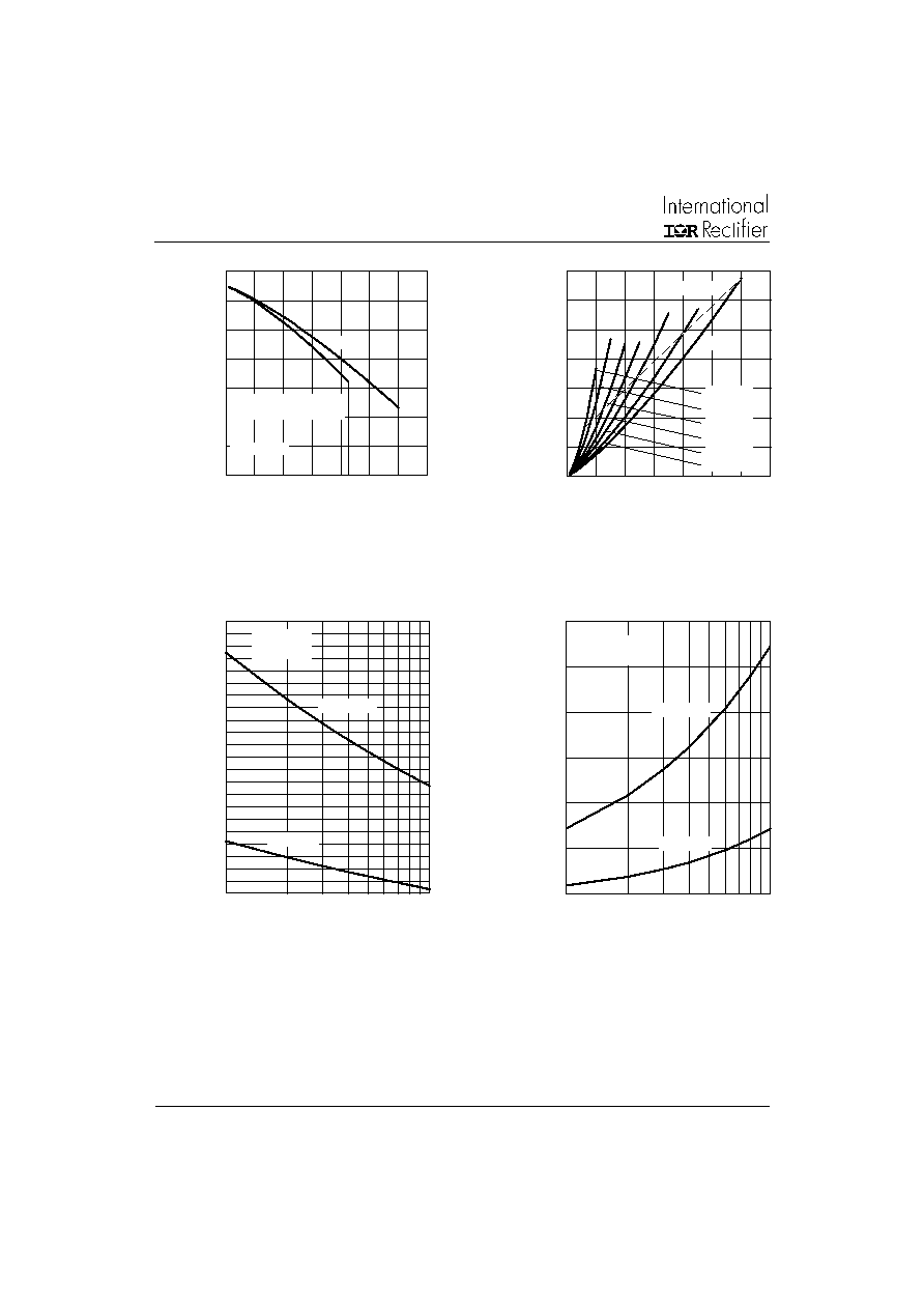
Fig. 5 - Max. Allowable Case Temperature
Vs. Average Forward Current (per diode)
Fig. 6 - Forward Power Loss (per diode)
(3) Formula used: T
C
= T
J
- (Pd + Pd
REV
) x R
thJC
;
Pd = Forward Power Loss = I
F(AV)
x V
FM
@ (I
F(AV)
/
D) (see Fig. 6);
Pd
REV
= Inverse Power Loss = V
R1
x I
R
(1 - D); I
R
@ V
R1
= 80% rated V
R
Average Power Loss ( Watts )
trr ( ns )
Qrr ( nC )
Average Forward Current - I
F(AV)
(A)
Allowable Case Temperature (°C)
Average Forward Current - I
F(AV)
(A)
di
F
/dt (A/µs )
di
F
/dt (A/µs )
Fig. 8 - Typical Stored Charge vs. di
F
/dt
Fig. 7 - Typical Reverse Recovery time vs. di
F
/dt
20
40
60
80
100
120
140
160
0
10
20
30
40
50
60
70
DC
Square wave (D = 0.50)
80% Rated Vr applied
see note (3)
0
10
20
30
40
50
60
70
0
10
20
30
40
50
60
70
DC
RMS Limit
D = 0.01
D = 0.02
D = 0.05
D = 0.10
D = 0.20
D = 0.50
50
60
70
80
90
100
110
120
130
140
150
160
100
1000
Tj = 125°C
Tj = 25°C
If = 50A
Vrr = 200V
50
550
1050
1550
2050
2550
3050
100
1000
Tj = 125°C
Tj = 25°C
If = 50A
Vrr = 200V
Bulletin PD-20488 12/01
UFB120FA40
5
www.irf.com
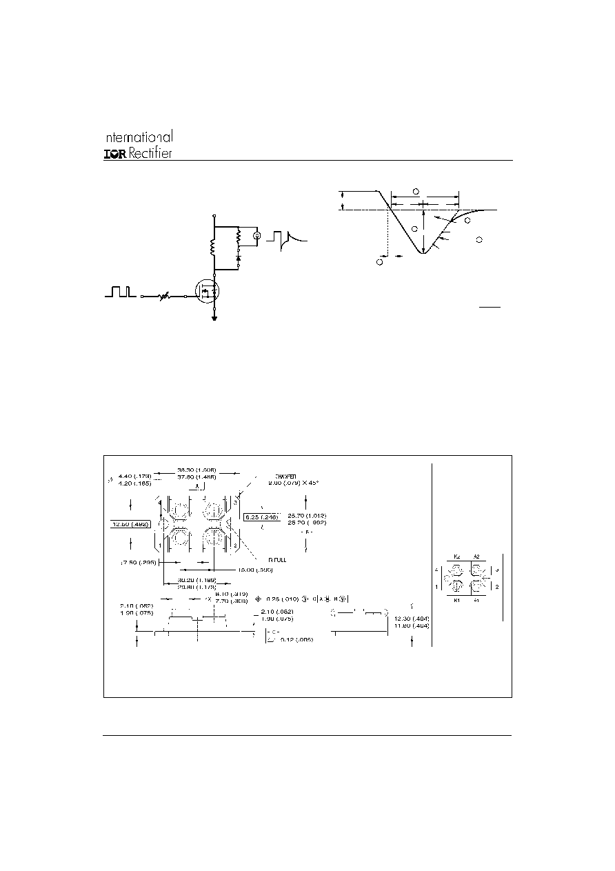
Fig. 2 - Reverse Recovery Waveform and
Definitions
Fig. 1 - Reverse Recovery Parameter Test
Circuit
IRFP250
D.U.T.
L = 70µH
V = 200V
R
0.01
G
D
S
dif/dt
ADJUST
4. Q
rr
- Area under curve defined by
t
rr
and I
RRM
5. di
(rec) M
/ dt - Peak rate of change
of current during t
b
portion of t
rr
1. di
F
/dt - Rate of change of current through
zero crossing
2. I
RRM
- Peak reverse recovery current
3. t
rr
- Reverse recovery time measured from
zero crossing point of negative going I
F
to
point where a line passing through 0.75 I
RRM
and 0.50 I
RRM
extrapolated to zero current
Q
rr =
t rr x I
RRM
2
t
a
t
b
t
rr
Q
rr
I
F
I
RRM
I
RRM
0.5
di(rec)M/dt
0.75 I
RRM
5
4
3
2
0
1
di /dt
f
SOT-227 Package Details
1. Dimensioning & tolerancing per ANSI Y14.5M-1982.
2. Controlling dimension: millimeter.
3. Dimensions are shown in millimeters (inches).
Notes:
FRED
LEAD ASSIGNMENTS