 | –≠–ª–µ–∫—Ç—Ä–æ–Ω–Ω—ã–π –∫–æ–º–ø–æ–Ω–µ–Ω—Ç: Z2803R5 | –°–∫–∞—á–∞—Ç—å:  PDF PDF  ZIP ZIP |
08/14/03
www.irf.com
1
LOW VOLTAGE
HIGH EFFICIENCY
RADIATION HARDENED
DC/DC CONVERTER
Z-ZERIES
Description
n
Output Voltages from 1.5 to 3.3 Volts
n
20 Amps Output Current
n
Synchronous Rectification
n
Efficiency up to 88%
n
Nominal 28 Volt Input
n
Total Ionizing Dose > 100KRad (Si)
n
No SEE to LET > 80 MeV
∑
cm
2
/mg
n
-40∞C to +85∞C Operating Range
n
Short Circuit Protection
n
Remote Sensing
n
Adjustable Output Voltage
n
Flexible Mounting Configuration
n
High Power Density
n
Derating To MIL-STD-975, MIL-STD-1547,
GSFC-PPL-21
n
Fully Isolated - Input to Output and to Case
n
Complimentary EMI Filter Available
n
Base Plate Conduction Cooling
Features
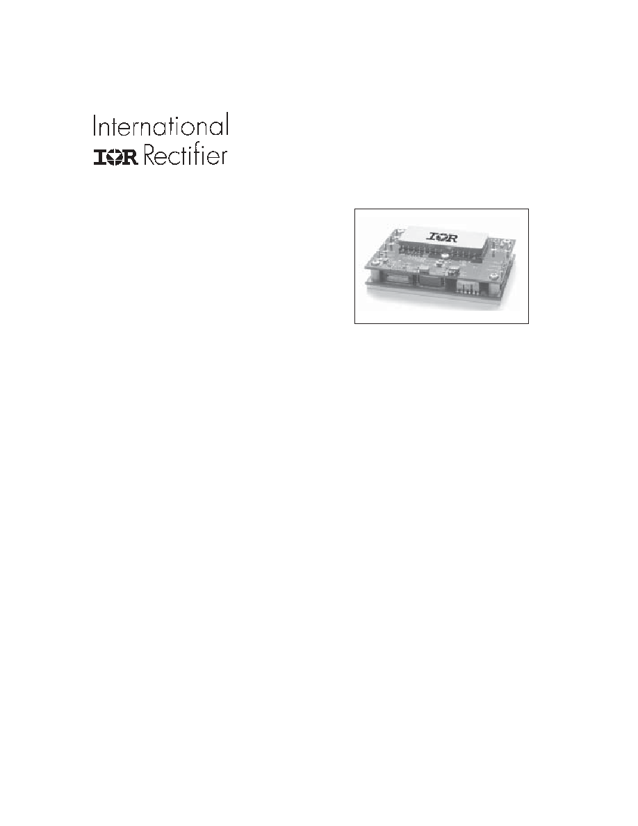
28V Input, Single Output
The Z-Series of DC/DC converter modules has been
specifically designed in response to the need for low
voltage at moderate current levels supplied with the
high efficiency and tight regulation dictated by modern
digital processing applications. These converters are
designed specifically for operation in radiation environ-
ments that are presented to commercial communica-
tion satellites operating in long term GEO and LEO or-
bits. They have been created to complement the spec-
trum of electrical and radiation performance available
in the Advanced Analog ART2815T and M3G-Series
converters. Requirements occurring in space vehicles
operating in Geostationary orbits, launch boosters, sci-
entific space probes and similar applications requiring
a low voltage, high efficiency converter with well char-
acterized radiation hardness performance will be opti-
mally satisfied by the Z-Series converters.
An additional benefit of the Z-Series is high power den-
sity. This is facilitated by utilizing the best features of
chip and wire hybrid technology and surface mount fab-
rication techniques. The hybrid portion is fabricated in
a facility fully qualified to MIL-PRF-38534 and pro-
cessed to class K requirements. The standard process-
ing adopted for the Z-Series module has been created
to assure with margin the reliability required for space
applications. Applicable generic lot qualification test
data including radiation performance will be made avail-
able on request. Variations to the standard screening
may be accommodated. Consult IR Santa Clara for
special requirements.
PD- 94693A

2
www.irf.com
Z-SERIES
Circuit Description
The Z-Series converters utilize a single ended forward
topology with resonant reset. The nominal 250kHz switch-
ing frequency has been selected to optimize magnetic
element size and switching loss. Electrical isolation be-
tween the primary and secondary sides of the converter
is assured through exclusive use of magnetic coupling for
all signals crossing the primary/secondary barrier. Volt-
age feed-forward is utilized to provide high line rejection.
An under-voltage lockout circuit prohibits the converter
from operating when the line voltage is too low to maintain
the output voltage. The converter will not start until the line
voltage rises to approximately 16.5 volts and will shut down
when the input voltage drops below 15.5 volts. This hys-
teresis voltage reduces the possibility of line noise inter-
fering with the converter's start-up and shut down. An
input overvoltage circuit is also in place that will shut down
the converter if the input voltage exceeds approximately
60 V, thereby precluding the possibility of exceeding the
voltage rating of the synchronous rectifiers.
A voltage of 0.8V or less will cause the converter to shut-
down. The pin may be left open for normal operation and
has a nominal open circuit voltage of 4.0V.
To achieve the high efficiencies characterizing these con-
verters, synchronous rectifiers have been used in place
of rectifying diodes thus minimizing the conduction losses
associated with those elements.
An internal EMI filter reduces the conducted emissions on
the input power leads. A two-stage output filter reduces
the typical output fundamental ripple to less than 20mV
peak-to-peak.
Output current is limited under any load fault condition to
approximately 125% of rated. An overload condition causes
the converter output to behave like a constant current
source with the output voltage dropping below nominal.
The converter will resume normal operation when the load
current is reduced below the current limit point. This pro-
tects the converter from both overload and short circuit
conditions. The current limit point exhibits a slightly nega-
tive temperature coefficient to reduce the possibility of
thermal runaway.
A synchronization input is provided allowing operation of
the converter synchronously with a user provided fre-
quency source. This input permits synchronization of the
converter to any compatible external frequency source
operating in the band of 225 to 300 KHz and is edge
triggered with synchronization initiated on the negative
transition. This signal should be a negative going pulse
referenced to the input return and have a 20% to 80%
duty cycle. Compatibility requires the negative transition
time to be less than 100 ns with minimum pulse amplitude
of +4.25 volts referred to the input return. In the event of
failure of an external synchronization source, the con-
verter will revert to its own internally set frequency. When
external synchronization is not desired, the sync input
may be left open (unconnected) permitting the converter
to operate at its' own internally set frequency.
An output adjust pin is provided permitting the user to
adjust the output voltage by approximately ± 5%. Adjust-
ment is accomplished by connecting a resistor brtween
the adjust pin (Pin 10) and +Sense (Pin 9) or ≠Sense (Pin
11). The direction of the output change is opposite the
sign of the sense pin to which it is connected, that is
connecting to the ≠ Sense pin causes an increase and
connecting to the +sense pin causes a decrease in output
voltage.
Remote sense is provided to compensate for conduction
losses in the connections between the converter outputs
and the load. The use of this sense feature permits com-
pensating for as much as 250 mV in both the output and
return lines. (500 mV each leg, round trip)
An external inhibit port is provided to control converter
operation. The nominal threshold relative to the input re-
turn (pin 2) is 1.4V. If 2.0 volts or greater are applied to the
Inhibit pin (pin 3) then the converter will operate normally.
Design Methodology
The Z-Series was developed using a proven conserva-
tive design methodology that includes selecting radiation
tolerant and established reliability components and fully
derating to the requirements of GSFC PPL-21, MIL-STD-
975 and MIL-STD-1547. Heavy derating of the radiation-
hardened power MOSFET virtually eliminates the possi-
bility of SEGR and SEB. A magnetic feedback circuit is
utilized instead of opto-couplers to minimize temperature,
radiation and aging sensitivity. PSPICE was used exten-
sively to predict and optimize circuit performance for both
beginning and end-of-life. Thorough design analyses in-
clude Worst Case, Stress, Thermal and Reliability (MTBF)
.
www.irf.com
3
Z-SERIES
For Notes to Specifications, refer to page 4
*
Exceeding maximum rating limits may cause damage to the device
Electrical Characteristics
-
40∞C
TBASE
+85∞C, VIN=28 VDC
±
5%, C
L
=0, unless otherwise specified.
Absolute Maximum Ratings*
Recommended Operating Conditions
Input Voltage
-0.5V to +50VDC
Input Voltage Range
+18V to +40V
Soldering
300∞C, 10 Sec
Output Power
0 to Max rated
Temperature Range Operating -40∞C to +85∞C Base Plate
Storage -55∞C to +105∞C Ambient
Base Plate
Temperature
-40∞C to +85∞C
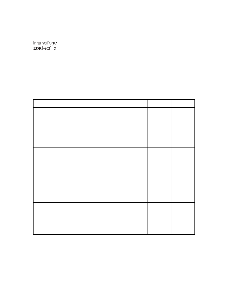
Parameter
Group A
Subgroups
Test
Conditions
Min
Nom
Max
Unit
Input Voltage
18
28
40
V
Output Voltage
Z2801R5S
Z2802R5S
Z2803R3S
Z2801R5S
Z2802R5S
Z2803R3S
1
1
1
2, 3
2, 3
2, 3
Iout = 0
1.485
2.475
3.267
1.470
2.450
3.234
1.500
2.500
3.300
1.515
2.525
3.333
1.530
2.550
3.366
V
V
V
V
V
V
Output Current
1
Z2801R5S
Z2802R5S
Z2803R3S
1, 2, 3
1, 2, 3
1, 2, 3
Vin = 18, 28, 40 Volts
20
20
15
A
A
A
Output Power
1
Z2801R5S
Z2802R5S
Z2803R3S
100% load
30
50
50
W
W
W
Output Ripple Voltage
2
Z2801R5S
Z2802R5S
Z2803R3S
1, 2, 3
1, 2, 3
1, 2, 3
Vin = 18, 28, 40 Volts
BW = 20 Hz to 2 MHz
20
30
40
mV
PP
mV
PP
mV
PP
Output Voltage
Regulation
3
Line
Load
1, 2, 3
1, 2, 3
Vin = 18, 28, 40 Volts
Iout = 10%, 50%, 100% load
±0.5
±0.5
%
%
Output Voltage
Temperature Coefficient
±0.02 %/∞C
4
www.irf.com
Z-SERIES
Electrical Characteristics
(Continued) -40∞C
TBASE
+85∞C, VIN=28 VDC
±
5%, C
L
=0, unless otherwise specified.
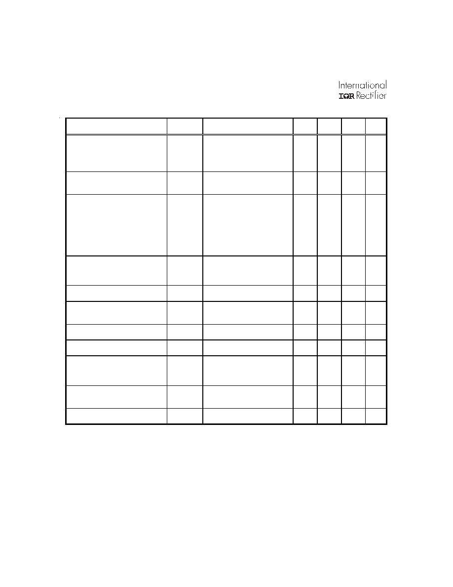
Notes to Specifications
1. Some parameters are not directly measured but are verified as part of another test
2. Measurement guaranteed for a bandwidth of 20 MHz. Tested with a bandwidth of 20KHz to 2MHz.
3. Regulation measured for all combinations of line and load conditions shown. Worst limit is presented for
each parameter.
Parameter
Group A
Subgroups
Test
Conditions
Min
Nom
Max
Unit
Input Current
No Load
Inhibited
1, 2, 3
1, 2, 3
Iout=0, Inhibit =open
Inhibit shorted to input return
5
500
14
mA
mA
Input Ripple Current
2
1, 2, 3
Vin = 18, 28, 40 Volts, 100%
load, BW = 20 Hz to 2 MHz
50
mA
PP
Efficiency
Z2801R5S
Z2802R5S
Z2803R3S
Z2801R5S
Z2802R5S
Z2803R3S
1
1
1
2, 3
2, 3
2, 3
100% load
79
83
85
78
82
84
80
85
88
%
%
%
%
%
%
Isolation
1
Input to output or any pin to
case (except case ground pin)
at 500Vdc
100
M
Capacitive Load
4
No effect on DC performance
2000
µF
Short Circuit Power Dissipation
1, 2, 3
19
w
Switching Frequency
4, 5, 6
100% load
225
250
275
KHz
Sync Frrequency Range
4, 5, 6
100% load
225
300
KHz
Turn-on Characteristics
Delay
Overshoot
1, 2, 3
1, 2, 3
30
10
mS
%
MTBF
MIL-HDBK-217F, N2
SF @ T
B
= 35∫C
3.96
Mhrs
Weight
200
g
www.irf.com
5
Z-SERIES
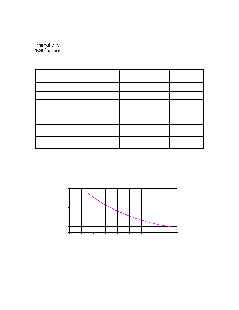
Flight Screening for Z-Series
Typical MTBF for Z-Series
MTBF vs Temperature
0.00
1.00
2.00
3.00
4.00
5.00
6.00
7.00
0
10
20
30
40
50
60
70
80
90
Base Plate Temperature
MTBF (10E6) Hr
s
Test
No.
Description
Conditions
Comments
1.
100% Full Functional Electrical Test (Group A)
25∞C (Subgroup 1) only
2.
100% Temperature Cycle, Operational
-40∞C to +100∞C, 5 Cycles
Record V
in
, I
in
and V
out
3.
100% Full Functional Electrical Test (Group A)
25∞C (Subgroup 1) only
4.
Sample Group A, Min, Max temperature
-40∞C, +85∞C (Subgroups 2, 3)
Sample 5(0)
5.
100% Burn-in
+85∞C Baseplate, 96 Hours
6.
100% Random Vibration, 3-Axis operational
MIL-STD-883, Method 2026,
Cond 1G, 1 minute each axis
Record V
in
, I
in
and V
out
7.
100% Full Functional Electrical Test (Group A)
3 temperature
-40∞C, +25∞C, +85∞C
(Subgroups 1, 2, 3)
Read and record data