Transistor
SERIES
Transistor With Resistor
For Switching Application
Silicon PNP Epitaxial Type
DESCRIPTION
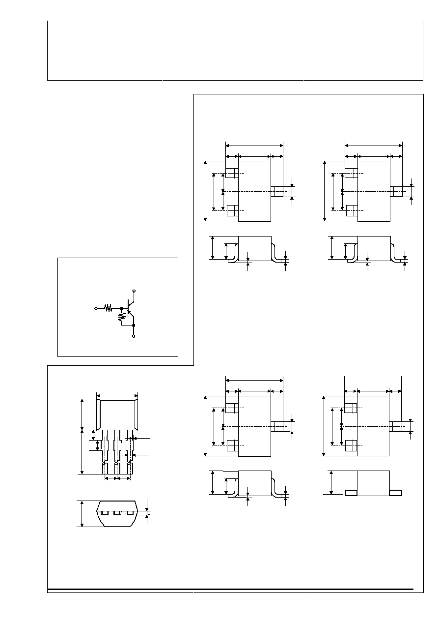
OUTLINE DRAWING UNITmm
RT1P141U
RT1P141C
RT1P141X is a one chip transistor
with built-in bias resistor,NPN type is RT1N141X.
FEATURE
Built-in bias resistor (R1=10k,R2=10k).
APPLICATION
Inverted circuit,switching circuit,interface circuit,
driver circuit.
Equivalent circuit
JEITA
JEDEC
JEITASC-59
JEDECSimilar to TO-236
Terminal Connector
Base
Emitter
Collector
Terminal Connector
Base
Emitter
Collector
RT1P141M
RT1P141T
JEITASC-70
JEDEC
JEITA
JEDEC
RT1P141S
Terminal Connector
Base
Emitter
Collector
Terminal Connector
Base
Emitter
Collector
0.15
0
0.1
0.55
0.7
0.3
0.4
0.8
0.4
1.6
0.5
0.5
1.0
1.6
0.16
0
0.1
0.8
1.1
0.4
0.5
1.5
0.5
2.5
0.95
0.95
1.90
2.9
0.15
0
0.1
0.7
0.9
0.3
1.25
0.425
2.1
0.65
0.65
1.3
2.0
0.425
4.0
1.0
1.0
14.0
3.0
1.27 1.27
0.45
0.1
2.5
0.4
C
(OUT)
E
(GND)
B
(IN)
R1
R2
ISAHAYA ELECTRONICS CORPORATION
JEITA
JEDEC
Emitter
Collector
Base
0.45
0.25
0.2
0.8
0.2
0.4
0.4
0.8
1.2

Transistor
SERIES
Transistor With Resistor
For Switching Application
Silicon PNP Epitaxial Type
MAXIMUM RATING (Ta=25)
RATING
SYMBOL
PARAMETER
RT1P141T
RT1P141U
RT1P141M
RT1P141C
RT1P141S
UNIT
Collector to Base voltage
-50
V
Emitter to Base voltage
-10
V
Collector to Emitter voltage
-50
V
Collector current
-100
mA
Peak Collector current
-200
mA
Collector
dissipation(Ta=25)
125
125
150
450
mW
Junction temperature
+125
+150
Storage temperature
-55+125
-55+150
ELECTRICAL CHARACTERISTICS (Ta=25)
package mounted on 9mm◊19mm◊1mm glass-epoxy substrate.
LIMIT
SYMBOL
PARAMETER
TEST CONDITION
MIN
TYP
MAX
UNIT
C to E break down voltage
I
C
=-100AR
BE
=
-50
V
Collector cut off current
V
CB
=-50VI
E
=0
-0.1
A
DC forward current gain
V
CE
=-5VI
C
=-10mA
50
C to E saturation voltage
I
C
=-10mAI
B
=-0.5mA
-0.1
-0.3
V
Input on voltage
V
CE
=-0.2VI
C
=-5mA
-1.5
-3.0
V
Input off voltage
V
CE
=-5VI
C
=-100A
-0.8
-1.1
V
Input resistance
7.0
10
13
k
Resistance ratio
0.9
1.0
1.1
Gain band width product
V
CE
=-6VI
E
=10mA
150
MHz
TYPICAL CHARACTERISTICS
ISAHAYA ELECTRONICS CORPORATION
Input On Voltage - Collector Current
-0.1
-1
-10
-1
-10
-100
Collector Current
In
pu
t
On
V
o
l
ta
ge
Collector Current - Input Off Voltage
-10
-100
-1000
-0
-0.4
-0.8
-1.2
-1.6
-2
Input Off Voltage
C
o
l
l
e
c
t
o
r
C
ur
re
nt
DC Forward Gain - Collector Current
1
10
100
1000
-1
-10
-100
Collector Current
DC
F
o
r
wa
r
d
G
a
i
n
Marketing division, Marketing planning department
6-41 Tsukuba, Isahaya, Nagasaki, 854-0065 Japan
Keep safety first in your circuit designs!
∑
ISAHAYA Electronics Corporation puts the maximum effort into making semiconductor products better and more reliable, but
there is always the possibility that trouble may occur with them. Trouble with semiconductors may lead to personal injury, fire or
property damage. Remember to give due consideration to safety when making your circuit designs, with appropriate measures
such as (1) placement of substitutive, auxiliary, (2) use of non-farmable material or (3) prevention against any malfunction or
mishap.
Notes regarding these materials
∑
These materials are intended as a reference to our customers in the selection of the ISAHAYA products best suited to the
customer's application; they don't convey any license under any intellectual property rights, or any other rights, belonging
ISAHAYA or third party.
∑
ISAHAYA Electronics Corporation assumes no responsibility for any damage, or infringement of any third party's rights ,
originating in the use of any product data, diagrams, charts or circuit application examples contained in these materials.
∑
All information contained in these materials, including product data, diagrams and charts, represent information on products
at the time of publication of these materials, and are subject to change by ISAHAYA Electronics Corporation without notice
due to product improvements or other reasons. It is therefore recommended that customers contact ISAHAYA Electronics
Corporation or an authorized ISAHAYA products distributor for the latest product information before purchasing product listed
herein.
∑
ISAHAYA Electronics Corporation products are not designed or manufactured for use in a device or system that is used
under circumstances in which human life is potentially at stake. Please contact ISAHAYA electronics corporation or an
authorized ISAHAYA products distributor when considering the use of a product contained herein for any specific purposes ,
such as apparatus or systems for transportation, vehicular, medical, aerospace, nuclear, or undersea repeater use.
∑
The prior written approval of ISAHAYA Electronics Corporation is necessary to reprint or reproduce in whole or in part these
materials.
∑
If these products or technologies are subject to the Japanese export control restrictions, they must be exported under a
license from the Japanese government and cannot be imported into a country other than the approved destination. Any
diversion or re-export contrary to the export control laws and regulations of Japan and/or the country of destination is
prohibited.
∑
Please contact ISAHAYA Electronics Corporation or authorized ISAHAYA products distributor for further details on these
materials or the products contained therein.
Jan.2003