
Integrated Silicon Solution, Inc. -- 1-800-379-4774
1
REV. A
11/01/01
ISSI
Æ
IS23SC4418
IS23SC4428
ISSI
Æ
ISSI reserves the right to make changes to its products at any time without notice in order to improve design and supply the best possible product. We assume no responsibility for any errors
which may appear in this publication. © Copyright 1999, Integrated Silicon Solution, Inc.
IS23SC4418
IS23SC4428
1-KBYTE EEPROM
WITH WRITE PROTECT FUNCTION AND
PROGRAMMABLE SECURITY CODE (PSC)
NOVEMBER 2001
FEATURES
∑ Standard CMOS process
∑ 1024 x 8 bits EEPROM organization
∑ Byte-wise addressing
∑ Byte-wise erase/write
∑ Irreversible byte-wise write protection
∑ Single 5V power supply for read and write/erase
∑ Low power operation:
≠ 3 mA typical active current
∑ 5 ms programming time
∑ 3-wire serial interface
∑ 20 KHz serial clock rate
∑ Contact configuration and serial interface,
ISO standard 7816 (Synchronous Transmission)
compatible.
∑ High ESD protection: > 4 KV
∑ High reliability:
≠ 1,000,000 erase/write cycles guaranteed
≠ 10 years data retention
∑ Wide operating temperature range
≠ 0 to +70∞C Commercial; ≠40 to +85∞C Industrial
Additional feature of IS23SC4428:
∑ 2-byte Programmable Security Code (PSC) for
memory write/erase protection
DESCRIPTION
IS23SC4418
IS23SC4418 contains 1024 x 8 bits of EEPROM with
programmable write protection for each byte. Random
read access to any byte in the memory is always possible.
The memory can also be erased and written byte by byte.
Erasing old data in the byte location must be performed
before new data can be written to the location. Each byte
in the memory has a corresponding protect bit. The
protect bits are only one-time programmable and cannot
be erased. After the protect bits are enabled (logic 0), the
corresponding bytes can never be changed again. A write-protect
bit with data-compare function is available for user to
verify the data in the memory before enabling the protect bit.
IS23SC4428
IS23SC4428 offers all the features in IS23SC4418. In
addition, it offers two bytes of Programmable Security
Code (PSC) against unauthorized memory write/erase
operations. All the memory, except for the PSC can
always be read, but the memory can be written or erased
only after PSC verification. If the user fails to enter the
correct PSC in eight consecutive attempts, the device will
block any further PSC entry attempts and the memory can
never be erased or written again.
The PSC bytes are pre-programmed by the manufacturer
with a code, which is specified for the customer for device
transport security purposes, before the devices are shipped
to the customer. The Error Counter will be pre-erased by
the manufacturer to allow maximum attempts (maximum
of eight) for PSC entry.
ISSI
Æ
2
Integrated Silicon Solution, Inc. -- 1-800-379-4774
REV. A
11/01/01
IS23SC4418
IS23SC4428
ISSI
Æ
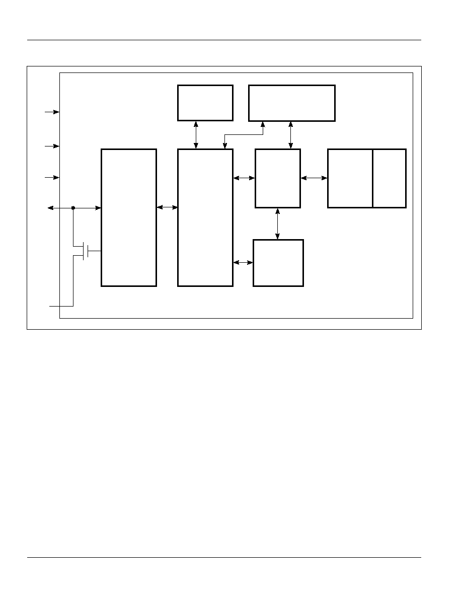
GND
I/O
CLK
RESET,
BLOCKADE
LOGIC
HIGH-VOLTAGE GENERATOR,
SUBSTATE-CURRENT
GENERATOR
SENSE AMP
AND
COMPARATOR
1024 X 8
EEPROM
WITH
DECODER
1024
PROTECT
BITS
(OTP)
PROGRAMMING
CONTROL
SEQUENCER
AND
SECURITY
LOGIC
INTERFACE
RST
Vcc
Figure 1. Block Diagram
Integrated Silicon Solution, Inc. -- 1-800-379-4774
3
REV. A
11/01/01
ISSI
Æ
IS23SC4418
IS23SC4428
ISSI
Æ
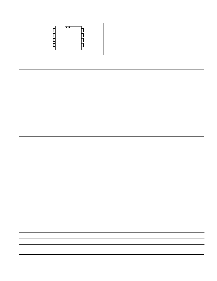
PIN NAMES
Pin
Card Contact
Symbol
Description
1
C1
Vcc
Supply Voltage
2
C2
RST
Reset
3
C3
CLK
Serial Clock
4
C4
NC
No Connect
5
C5
GND
Ground
6
C6
NC
No Connect
7
C7
I/O
Serial Data I/O (open drain)
8
C8
NC
No Connect
C1
C2
C3
C4
C5
C6
C7
C8
Vcc
RST
CLK
NC
GND
NC
I/O
NC
PIN DESCRIPTIONS
Symbol
Type
Card Contact
Name and Function
Vcc
C1
Supply Voltage
RST
C2
Reset: The device reset pin (RST) is used to take the device out of the power-on
reset state (POR). When the operating power is first applied to Vcc, the device goes
into POR state. The POR state can be terminated by RST in this sequence: bring
RST from 0 to 1 and then change CLK from 0 to 1 (See Figure 3). This reset
operation terminates any active command operation. After the POR state has been
terminated, a read operation must be performed before any data can be erased or
written. Also, IS23SC4418/28 meets the ISO 7816 specification on Answer to Reset
function. The Answer to Reset can be invoked by performing the following steps:
1) RST goes from 0 to 1; 2) CLK pulse is applied; 3) RST changes from 1 to 0.
If these steps are performed correctly, the device will set the address counter to 0
and the first data bit at byte address 0 will appear on the output (I/O). By continuing
to send pulses at CLK, the contents of the following byte addresses can be read out
of the device. (See Figure 3)
In normal operation, RST controls the data input and output directions. When
sending data/command to the device, RST is set to 1. When reading data/PSC
verification output from the device, RST is set to 0. (See Figure 4)
CLK
C3
Serial Clock: This is the device data clock pin. It is used to clock data bits into and
out of the device.
NC
C4, C6, C8
No Connect
GND
C5
Ground
I/O
C7
Serial Data Input and Output: This pin is where data is shifted in and out of the
device.
Figure 2. Pin Configuration

4
Integrated Silicon Solution, Inc. -- 1-800-379-4774
REV. A
11/01/01
IS23SC4418
IS23SC4428
ISSI
Æ
VCC
Bit1
Bit2
Bit31
Bit32
32
2
1
RST
t
ARE
t
RSTS1
t
RSTH
t
D
t
DH
t
H
CLK
I/O
t
L
Figure 3. Reset and Answer to Reset Timing Diagram
Figure 4. General Timing for Data Input, Data Output and PSC Verification
Data Input
Data Output
or PSC Verification
RST
CLK
Bit0
0
1
t
RE
t
DS
t
DH
23
Bit1
Bit23
Bit0
0
1
2
3
Bit1
Bit2
I/O
t
H
t
RSTH
t
RSTS2
t
DH
t
L

Integrated Silicon Solution, Inc. -- 1-800-379-4774
5
REV. A
11/01/01
ISSI
Æ
IS23SC4418
IS23SC4428
ISSI
Æ
Table 1. Control Words for IS23SC4418/4428 Commands
Command Name
Byte 1
Byte 2
Byte 3
S0 S1 S2 S3 S4 S5
A8 A9
A0-A7
D0-D7
Read 8-bits data without protect bit
0
1
1
1
0
0
A8 A9
A0-A7
Don't Care
Read 9-bits data with protect bit
0
0
1
1
0
0
A8 A9
A0-A7
Don't Care
Write and erase without protect bit
(1)
1
1
0
0
1
1
A8 A9
A0-A7
Input data
Write and erase with protect bit
(1)
1
0
0
0
1
1
A8 A9
A0-A7
Input data
Write protect bit with data comparison
(1)
0
0
0
0
1
1
A8 A9
A0-A7
Compare data
Additional Commands for IS23SC4428 only
(3)
Write Error Counter
0
1
0
0
1
1
1
1
FDH
Bit Mask
Verify first PSC byte
1
0
1
1
0
0
1
1
FEH
PSC byte 1
Verify second PSC byte
1
0
1
1
0
0
1
1
FFH
PSC byte 2
Write and erase first PSC byte
1
1
0
0
1
1
1
1
FEH
PSC byte 1
without protect bit
(2)
Write and erase second PSC byte
1
1
0
0
1
1
1
1
FFH
PSC byte 2
without protect bit
(2)
Write and erase first PSC byte
1
0
0
0
1
1
1
1
FEH
PSC byte 1
with protect bit
(2)
Write and erase second PSC byte
1
0
0
0
1
1
1
1
FFH
PSC byte 2
with protect bit
(2)
Read 8-bits first PSC byte
0
1
1
1
0
0
1
1
FEH
Don't Care
without protect bit
(2)
Read 8-bits second PSC byte
0
1
1
1
0
0
1
1
FFH
Don't Care
without protect bit
Read 9-bits first PSC byte
0
0
1
1
0
0
1
1
FEH
Don't Care
with protect bit
Read 9-bits second PSC byte
0
0
1
1
0
0
1
1
FFH
Don't Care
with protect bit
Notes:
1. If the protect bit of the byte address is enabled, the write command will have no effect on the byte content.
2. If the protect bit of the PSC byte is enabled, the write command will have no effect on the PSC byte.
3. For IS23SC4428, locations (1021-1023) are occupied by Error Counter and PSC codes and thus cannot be used for general data
storage.