
Integrated Silicon Solution, Inc. -- www.issi.com --
1-800-379-4774
1
Rev. D
06/25/02
IS24C01 IS24C02
IS24C04 IS24C08 IS24C16
ISSI
Æ
Copyright © 2002 Integrated Silicon Solution, Inc. All rights reserved. ISSI reserves the right to make changes to this specification and its products at any time
without notice. ISSI assumes no liability arising out of the application or use of any information, products or services described herein. Customers are advised to
obtain the latest version of this device specification before relying on any published information and before placing orders for products.
1K-bit/2K-bit/4K-bit/8K-bit/16K-bit
2-WIRE SERIAL CMOS EEPROM
APRIL 2002
DESCRIPTION
The IS24CXX (refers to IS24C01, IS24C02, IS24C04,
IS24C08, IS24C16) family is a low-cost and low voltage 2-
wire Serial EEPROM. It is fabricated using ISSI's advanced
CMOS EEPROM technology and provides a low power and
low voltage operation. The IS24CXX family features a write
protection feature, and is available in 8-pin DIP and 8-pin
SOIC packages.
The IS24C01 is a 1K-bit EEPROM; IS24C02 is a 2K-bit
EEPROM; IS24C04 is a 4K-bit EEPROM; IS24C08 is a 8K-
bit EEPROM; IS24C16 is a 16K-bit EEPROM.
The IS24C01 and IS24C02 are available in 8-pin MSOP
package. The IS24C01, IS24C02, IS24C04, and IS24C08
are available in 8-Pin TSSOP package.
Automotive data is preliminary.
FEATURES
∑ Low Power CMOS Technology
≠Standby Current less than 8 µA (5.5V)
≠Read Current (typical) less than 1 mA (5.5V)
≠Write Current (typical) less than 3 mA (5.5V)
∑ Flexible Voltage Operation
≠Vcc = 1.8V to 5.5V for ≠2 version
≠Vcc = 2.5V to 5.5V for ≠3 version
∑ 400 KHz (I
2
C Protocol) Compatibility
∑ Hardware Data Protection
≠Write Protect Pin
∑ Sequential Read Feature
∑ Filtered Inputs for Noise Suppression
∑ 8-pin PDIP and 8-pin SOIC packages
∑ 8-pin TSSOP (1K,2K, 4K & 8K only)
∑ 8-pin MSOP (1K,2K only)
∑ Self time write cycle with auto clear
5 ms @ 2.5V
∑ Organization:
≠IS24C01 128x8 (one block of 128 bytes)
≠IS24C02 256x8 (one block of 256 bytes)
≠IS24C04 512x8 (two blocks of 256 bytes)
≠IS24C08 1024x8 (four blocks of 256 bytes)
≠IS24C16 2048x8 (eight blocks of 256 bytes)
∑ Page Write Buffer
∑ Two-Wire Serial Interface
≠Bi-directional data transfer protocol
∑ High Reliability
≠Endurance: 1,000,000 Cycles
≠Data Retention: 100 Years
∑ Commercial, Industrial and Automotive tempera-
ture ranges
2
Integrated Silicon Solution, Inc. -- www.issi.com --
1-800-379-4774
Rev. D
06/25/02
IS24C01
IS24C02
IS24C04
IS24C08 IS24C16
ISSI
Æ
>
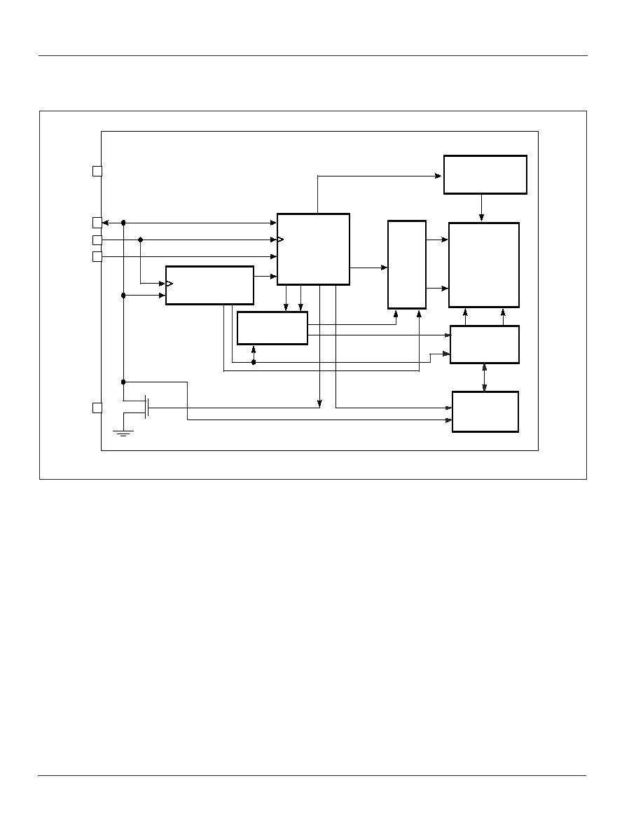
CONTROL
LOGIC
X
DECODER
SLAVE ADDRESS
REGISTER &
COMPARATOR
WORD ADDRESS
COUNTER
HIGH VOLTAGE
GENERATOR,
TIMING & CONTROL
EEPROM
ARRAY
Y
DECODER
DATA
REGISTER
Clock
DI/O
ACK
8
5
6
7
4
GND
WP
SCL
SDA
Vcc
nMOS
FUNCTIONAL BLOCK DIAGRAM
Integrated Silicon Solution, Inc. -- www.issi.com --
1-800-379-4774
3
Rev. D
06/25/02
IS24C01
IS24C02
IS24C04
IS24C08 IS24C16
ISSI
Æ
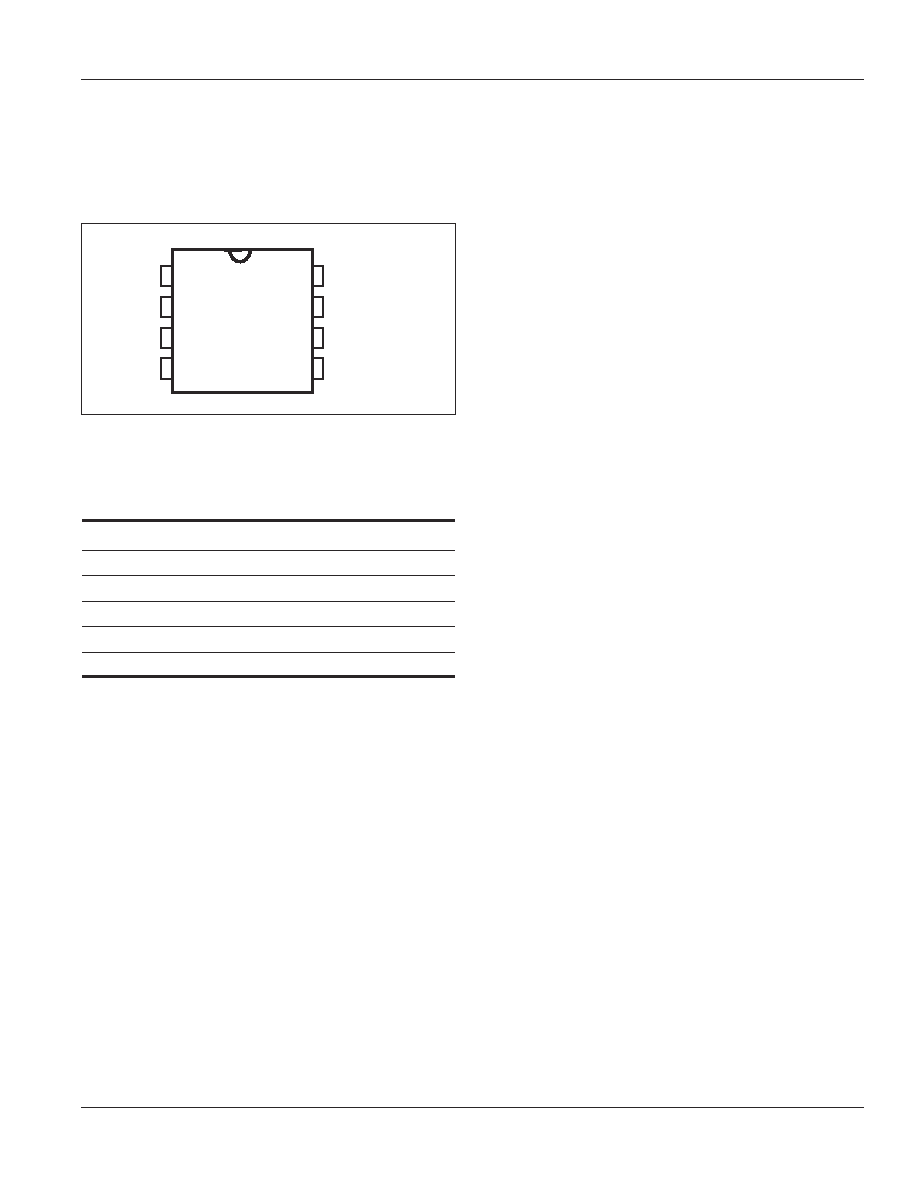
PIN DESCRIPTIONS
A0-A2
Address Inputs
SDA
Serial Address/Data I/O
SCL
Serial Clock Input
WP
Write Protect Input
Vcc
Power Supply
GND
Ground
SCL
This input clock pin is used to synchronize the data
transfer to and from the device.
SDA
The SDA is a Bi-directional pin used to transfer addresses and data
into and out of the device. The SDA pin is an open drain output and
can be wire-Ored with other open drain or open collector outputs.
The SDA bus
requires a pullup resistor to Vcc.
A0, A1, A2
The A0, A1 and A2 are the device address inputs. The IS24C01 and
IS24C02 use the A0, A1, and A2 for hardware addressing and a
total of 8 devices may be used on a single bus system.
PIN CONFIGURATION
8-Pin DIP and SOIC
8 Pin TSSOP (1K, 2K, 4K and 8K)
8-Pin MSOP (1K, 2K)
1
2
3
4
8
7
6
5
A0
A1
A2
GND
VCC
WP
SCL
SDA
The IS24C04 uses A1 and A2 pins for hardwire addressing and
a total of four devices may be addressed on a single bus system.
The A0 pin is not used by IS24C04. This pin can be left floating
or tied to GND or Vcc.
The IS24C08 only use A2 input for hardwire addressing and a
total of two devices may be addressed on a single bus system.
The A0 and A1 pins are not used by IS24C08. They may be left
floating or tied to either GND or Vcc.
These pins are not used by IS24C16. A0 and A1 may be left
floating or tied to either GND or Vcc. A2 should be tied to either
GND or Vcc.
WP
WP is the Write Protect pin. On the 24C01, 24C02, IS24C04
and 24C08, if the WP pin is tied to V
CC
the entire array
becomes Write Protected (Read only). On the 24C16, if the
WP pin is tied to Vcc the upper half array becomes Write
Protected (Read only). When WP is tied to GND or left
floating normal read/write operations are allowed to the
device.

4
Integrated Silicon Solution, Inc. -- www.issi.com --
1-800-379-4774
Rev. D
06/25/02
IS24C01
IS24C02
IS24C04
IS24C08 IS24C16
ISSI
Æ
DEVICE OPERATION
The IS24CXX family features a serial communication and
supports a bi-directional 2-wire bus transmission protocol.
2-WIRE BUS
The two-wire bus is defined as a Serial Data line(SDA), and
a Serial Clock Line (SCL). The protocol defines any device
that sends data onto the SDA bus as a transmitter, and the
receiving devices as a receiver. The bus is controlled by
MASTER device which generates the SCL, controls the bus
access and generates the STOP and START conditions.
The IS24CXX is the SLAVE device on the bus.
THE BUS PROTOCOL:
-- Data transfer may be initiated only when the bus is not
busy
-- During a data transfer, the data line must remain stable
whenever the clock line is high. Any changes in the data
line while the clock line is high will be interpreted as a
START or STOP condition.
The state of the data line represents valid data when after
a START condition, the data line is stable for the duration
of the HIGH period of the clock signal. The data on the line
must be changed during the LOW period of the clock signal.
There is one clock pulse per bit of data. Each data transfer
is initiated with a START condition and terminated with a
STOP condition.
START CONDITION
The START condition precedes all commands to the
devices and is defined as a HIGH to LOW transition of SDA
when SCL is HIGH. The IS24CXX monitors the SDA and
SCL lines and will not respond until the START condition is
met.
STOP CONDITION
The STOP condition is defined as a LOW to HIGH transition
of SDA when SCL is HIGH. All operations must end with a
STOP condition.
ACKNOWLEDGE
After a successful data transfer, each receiving device is
required to generate an acknowledge. The Acknowledging
device pulls down the SDA line.
DEVICE ADDRESSING
The MASTER begins a transmission by sending a START
condition. The MASTER then sends the address of the
particular slave devices it is requesting. The SLAVE
address is 8 bytes.
The four most significant bytes of the address are fixed as
1010 for the IS24CXX.
For the IS24C16, the bytes(B2, B1 and B0) are used for
memory page addressing (the IS24C16 is organized as
eight blocks of 256 bytes).
For the IS24C04 out of the next three bytes, B0 is for
Memory Page Addressing (the IS24C04 is organized as two
blocks of 256 bytes) and A2 and A1 bytes are used as
device address bytes and must compare to its hard-wire
inputs pins (A2 and A1). Up to four IS24C04's may be
individually addressed by the system. The page addressing
bytes for IS24Cxx should be considered the most significant
bytes of the data word address which follows.
For the IS24C08 out of the next three bytes, B1 and B0 are
for memory page addressing (the IS24C08 is organized as
four blocks of 256 bytes) and the A2 bit is used as device
address bit and must compare to its hard-wired input pin
(A2). Up to two IS24C08 may be individually addressed by
the system. The page addressing bytes for IS24CXX
should be considered the most significant bytes of the data
word address which follows.
For the IS24C01 and IS24C02, the A0, A1, and A2 are used
as device address bytes and must compare to its hard-
wired input pins (A0, A1, and A2) Up to Eight IS24C01 and/
or IS24C02's may be individually addressed by the system.
The last bit of the slave address specifies whether a Read
or Write operation is to be performed. When this bit is set
to 1, a Read operation is selected, and when set to 0, a Write
operation is selected.
After the MASTER sends a START condition and the
SLAVE address byte, the IS24CXX monitors the bus and
responds with an Acknowledge (on the SDA line) when its
address matches the transmitted slave address. The
IS24CXX pulls down the SDA line during the ninth clock
cycle, signaling that it received the eight bytes of data. The
IS24CXX then performs a Read or Write operation depending
on the state of the R/
W
bit.
WRITE OPERATION
BYTE WRITE
In the Byte Write mode, the Master device sends the
START condition and the slave address information(with
the R/
W
set to Zero) to the Slave device. After the Slave
generates an acknowledge, the Master sends the byte
address that is to be written into the address pointer of the
IS24CXX. After receiving another acknowledge from the
Slave, the Master device transmits the data byte to be
written into the address memory location. The IS24CXX
acknowledges once more and the Master generates the
STOP condition, at which time the device begins its internal
programming cycle. While this internal cycle is in progress,
the device will not respond to any request from the Master
device.

Integrated Silicon Solution, Inc. -- www.issi.com --
1-800-379-4774
5
Rev. D
06/25/02
IS24C01
IS24C02
IS24C04
IS24C08 IS24C16
ISSI
Æ
condition and the IS24CXX discontinues transmission. If
'n' is the last byte of the memory, then the data from location
'0' will be transmitted. (Refer to Current Address Read
Diagram.)
RANDOM ADDRESS READ
Selective READ operations allow the Master device to
select at random any memory location for a READ operation.
The Master device first performs a 'dummy' write operation
by sending the START condition, slave address and word
address of the location it wishes to read. After the IS24CXX
acknowledge the word address, the Master device resends
the START condition and the slave address, this time with
the R/
W
bit set to one. The IS24CXX then responds with its
acknowledge and sends the data requested. The master
device does not send an acknowledge but will generate a
STOP condition. (Refer to Random Address Read Diagram.)
SEQUENTIAL READ
Sequential Reads can be initiated as either a Current
Address Read or Random Address Read. After the IS24CXX
sends initial byte sequence, the master device now responds
with an ACKnowledge indicating it requires additional data
from the IS24CXX. The IS24CXX continues to output data
for each ACKnowledge received. The master device
terminates the sequential READ operation by pulling SDA
HIGH (no ACKnowledge) indicating the last data word to be
read, followed by a STOP condition.
The data output is sequential, with the data from
address n followed by the data from address n+1, ... etc.
The address counter increments by one automatically,
allowing the entire memory contents to be serially read
during sequential read operation. When the memory address
boundary (127 for IS24C01; 255 for IS24C02; 511 for
IS24C04; 1023 for IS24C08; 2047 for IS24C16) is reached,
the address counter "rolls over" to address 0, and the
IS24CXX continues to output data for each ACKnowledge
received. (Refer to Sequential Read Operation Starting with
a Random Address READ Diagram.)
PAGE WRITE
The IS24CXX is capable of page-WRITE (8-byte for 24C01/
02 and 16-byte for 24C04/08/16) operation. A page-WRITE
is initiated in the same manner as a byte write, but instead
of terminating the internal write cycle after the first data word
is transferred, the master device can transmit up to N more
bytes (N=7 for 24C01/02 and N=15 for 24C04/08/16). After
the receipt of each data word, the IS24CXX responds
immediately with an ACKnowledge on SDA line, and the
three lower (24C01/24C02) or four lower (24C04/24C08/
24C16) order data word address bits are internally
incremented by one, while the higher order bits of the data
word address remain constant. If the master device should
transmit more than N+1 (N=7 for 24C01/02 and N=15 for
24C04/08/16) words, prior to issuing the STOP condition,
the address counter will "roll over," and the previously
written data will be overwritten. Once all N+1 (N=7 for
24C01/02 and N=15 for 24C04/08/16) bytes are received
and the STOP condition has been sent by the Master, the
internal programming cycle begins. At this point, all received
data is written to the IS24CXX in a single write cycle. All
inputs are disabled until completion of the internal WRITE
cycle.
ACKNOWLEDGE POLLING
The disabling of the inputs can be used to take advantage
of the typical write cycle time. Once the stop condition is
issued to indicate the end of the host's write operation, the
IS24CXX initiates the internal write cycle. ACK polling can
be initiated immediately. This involves issuing the start
condition followed by the slave address for a write operation.
If the IS24CXX is still busy with the write operation, no ACK
will be returned. If the IS24CXX has completed the write
operation, an ACK will be returned and the host can then
proceed with the next read or write operation.
READ OPERATION
READ operations are initiated in the same manner as
WRITE operations, except that the read/write bit of the
slave address is set to "1". There are three READ operation
options: current address read, random address read and
sequential read.
CURRENT ADDRESS READ
The IS24CXX contains an internal address counter which
maintains the address of the last byte accessed, incremented
by one. For example, if the previous operation is either a
read or write operation addressed to the address location n,
the internal address counter would increment to address
location n+1. When the IS24CXX receives the Device
Addressing Byte with a READ operation (read/write bit set
to "1"), it will respond an ACKnowledge and transmit the 8-
bit data word stored at address location n+1. The master will
not acknowledge the transfer but does generate a STOP