 | –≠–ª–µ–∫—Ç—Ä–æ–Ω–Ω—ã–π –∫–æ–º–ø–æ–Ω–µ–Ω—Ç: IS24C16-P | –°–∫–∞—á–∞—Ç—å:  PDF PDF  ZIP ZIP |
ISSI
Æ
IS24C16
Integrated Silicon Solution, Inc.
1
ADVANCE INFORMATION
EE001-0C
10/03/97
This document contains ADVANCE INFORMATION data. ISSI reserves the right to make changes to its products at any time without notice in order to improve design and supply the best possible
product. We assume no responsibility for any errors which may appear in this publication. © Copyright 1997, Integrated Silicon Solution, Inc.
IS24C16
16,384-BIT SERIAL ELECTRICALLY
ERASABLE PROM
FEATURES
∑ Low power CMOS
≠ Active current less than 3.0 mA
≠ Standby current less than 35
µ
A
∑ Hardware write protection
≠ Write control pin
∑ Internally organized as eight banks
≠ 256 pages x 8 bytes
∑ Two-wire serial interface
-- Bidirectional data transfer protocol
∑ Flexible byte write and 16-byte page-write
modes
∑ High-reliability
≠ Endurance: 100,000 cycles per byte
≠ Data retention: 100 years
∑ Automatic word address incrementing
-- Sequential register read
∑ Filtered inputs for noise suppression
∑ 8-pin PDIP or SOIC packages
OVERVIEW
The IS24C16 is a low cost, low power, low voltage
serial EEPROM and organized as 2,048 x 8 bits. The
memory is configured as 128 pages of 16 bytes each. It is
fabricated using
ISSI
's advanced CMOS EEPROM tech-
nology and operates from a single supply.
The IS24C16 is internally organized as a 256 x 8 memory
bank. The IS24C16 features a serial interface and soft-
ware protocol allowing operation on a simple 2-wire bus.
Included is a bidirectional serial data bus synchronized by
a clock offering flexible byte write and a faster 16-byte
page write. A write protect pin can protect data in the upper
quadrant of memory.
ADVANCE INFORMATION
OCTOBER 1997
ISSI
Æ
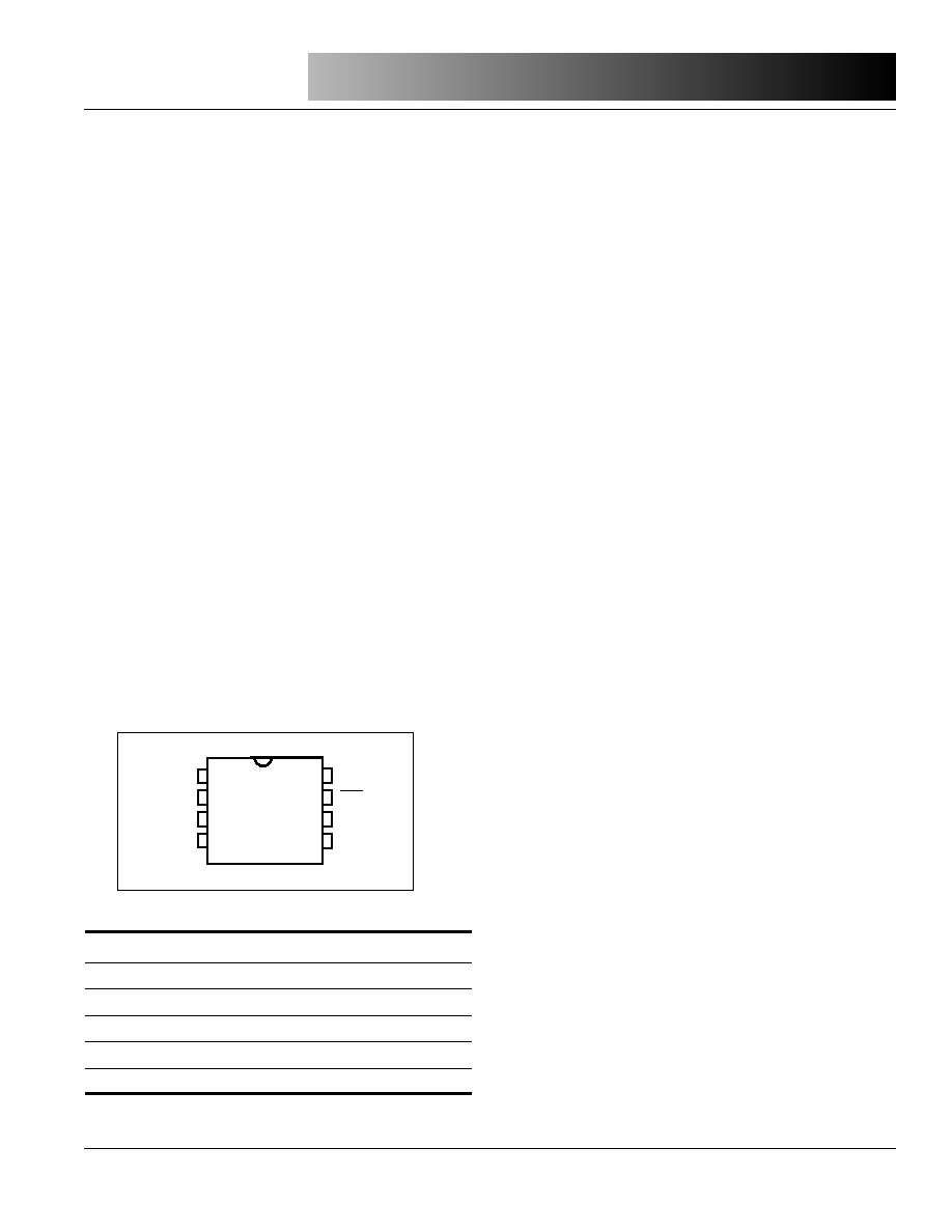
PIN CONFIGURATION
8-Pin DIP and SOIC
PIN DESCRIPTIONS
Serial Clock (SCL) - The SCL input is used to clock all data
into and out of the device. In the WRITE mode, data must
remain stable when SCL is HIGH. In the READ mode, data
is clocked out on the falling edge of SCL.
Serial Data (SDA) - The SDA pin is a bidirectional pin used
to transfer data into and out of the device. Data may
change only when SCL is LOW. It is an open-drain output,
and may be wire-ORed with any number of open-drain or
open-collector outputs.
A0, A1, and A2: These pins are not connected.
Write Control (
WC
WC
WC
WC
WC
) - The Write Control input is used to
disable any attempt to write to the memory. When HIGH,
the upper half of array is protected against write opera-
tions; when LOW, the write function is normal. The part can
be read independent of the state of
WC
pin. When not
connected this pin will be pulled LOW.
1
2
3
4
8
7
6
5
A0
A1
A2
GND
VCC
WC
SCL
SDA
PIN DESCRIPTIONS
A0-A2
Address Inputs (No connection)
SDA
Serial Data I/O
SCL
Serial Clock Input
WC
Write Control Input
Vcc
Power
GND
Ground

ISSI
Æ
IS24C16
2
Integrated Silicon Solution, Inc.
ADVANCE INFORMATION
EE001-0C
10/03/97
GENERAL DESCRIPTION
The IS24C16 features a SERIAL communication, and
supports bidirectional data transmission protocol allowing
one IS24C16 operation on a simple two-wire bus. The two-
wire bus is defined as a serial data line (SDA), and a serial
clock line (SCL). (Refer to Figure 1. Typical System Bus
Configuration.)
The protocol defines any device that sends data onto the
SDA bus as a transmitter, and the receiving device as a
receiver. The device controlling the data transmission is
named MASTER device, and the controlled device is
named SLAVE device.
The IS24C16 does not use any device address bits but
instead the three bits are used for memory page address-
ing. These page addressing bits should be considered the
most significant bits of the data word address which
follows. The A0, A1, and A2 pins are no connect.
The eighth bit of the device address is the read/write
operation select bit. A read operation is initiated if this bit
is HIGH and a write operation is initiated if this bit is LOW.
The ACKnowledge is used to indicate successful data
transfers. The transmitting device will release the data bus
(SDA goes HIGH) after transmitting eight bits (one data bit
is transfered at the falling edge of each clock cycle). During
the ninth clock cycle, the receiver will pull the SDA line
LOW to ACKnowledge the transmitter that it received the
eight bits of data. (Refer to Figure 2. ACKnowledge Re-
sponse from Receiver Diagram.)
DEVICE OPERATION
START and STOP Conditions
Both SDA and SCL lines remain HIGH when the SDA bus
is not busy. A HIGH-to-LOW transition of SDA line, while
SCL is HIGH, is defined as the START condition. A LOW-
to-High transition of SDA line, while SCL is HIGH, is
defined as the STOP condition. (Refer to Figure 3. Start
and Stop Conditions.)
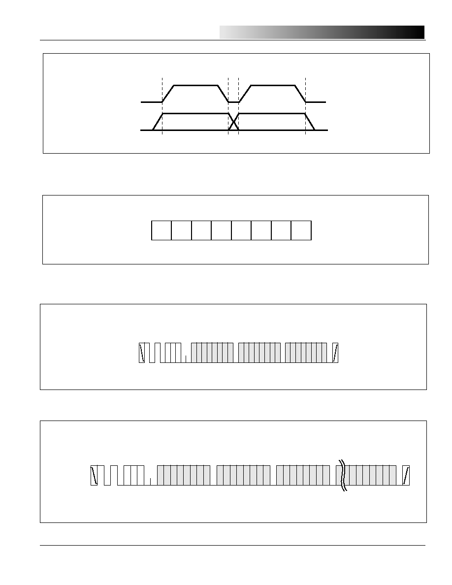
Data Validity Protocol
One data bit is transferred during each clock cycle. The
data on the SDA line must remain stable during the HIGH
period of the clock cycle, because changes on SDA line
during the SCL HIGH period will be interpreted as START
or STOP control signals. (Refer to Figure 4. Data Validity
Protocol.)
Device Addressing Byte Definitions
The most significant four bits of Device Addressing Byte
(Bit 7 to Bit 4) are defined as the device type identifier. For
IS24C16, this is fixed as 1010. The next three significant
address bits (Bit 3 to Bit 1) are address memory bits. One
IS24C16 device can be connected on the bus. The last bit
Bit 0 defines the write or read operation to be performed.
When set to "1", a READ operation is selected; when set
to "0" a WRITE operation is selected. (Refer to Figure 5.
Device Addressing Byte Definitions.)
WRITE OPERATION
Byte Write
For a WRITE operation, the IS24C16 requires another
8-bit data word address following the Device Addressing
Byte and ACKnowledgement. This data word address
provides access to any one of the 256 data words of
device's memory array.
Upon receipt of the data word address, the IS24C16
responds with an ACKnowledge on SDA, and waits for the
next 8-bit data word, then again responding with an
ACKnowledge. The master device terminates the Byte
Write Operation by generating a STOP condition, after-
ward the IS24C16 begins the internal WRITE cycle to the
nonvolatile memory array. Refer to Write Cycle Timing. All
inputs are disabled during this write cycle and the device
will not response to any requests from the master. (Refer
to Figure 6. Write Operation for the Address, ACKnowledge,
and Data Transfer Sequence.)
Page Write
The IS24C16 is capable of 8-byte page- WRITE operation.
A page-WRITE is initiated in the same manner as a byte
write, but instead of terminating the internal write cycle
after the first data word is transfered, the master device
can transmit up to 15 more words. After the receipt of each
data word, the IS24C16 responds immediately with an
ACKnowledge on SDA line, and the four lower order data
word address bits are internally incremented by one while
the four higher order bits of the data word address remain
constant. If the master device should transmit more than
8 words, prior to issuing the STOP condition, the address
counter will "roll over," and the previously written data will
be overwritten. All inputs are disabled until completion of
the internal WRITE cycle. (Refer to Figure 7. Write Opera-
tion for the Address, ACKnowledge, and Data Transfer
Sequence.)

ISSI
Æ
IS24C16
Integrated Silicon Solution, Inc.
3
ADVANCE INFORMATION
EE001-0C
10/03/97
Acknowledge Polling
Once the internal write cycle has started and the
IS24C16 inputs are disabled, acknowledge polling can be
initiated. This involves sending a start condition followed
by the Device Addressing Byte. The read/write bit is
representive of the operation desired. Only if the internal
write cycle has been completed will the IS24C16 respond
with an acknowledge on the SDA bus allowing the read or
write sequence to continue.
READ OPERATION
READ operations are initiated in the same manner as
WRITE operations, except that the read/write bit of the
device addressing byte is set to "1". There are three READ
operation options: current address read, random address
read and sequential read.
Current Address Read
The IS24C16 contains an internal address counter which
maintains the address of the last data word accessed,
incremented by one. For example, if the previous opera-
tion either a read or write operation addressed to the
address location n, the internal address counter would
increment to address location n+1. When the IS24C16
receives the Device Addressing Byte with a READ opera-
tion (read/write bit set to "1"), it will respond an ACKnowledge
and transmit the 8-bit data word stored at address location
n+1. If the Current Address READ operation only ac-
cesses a single byte of data, the master device terminates
the Current Address READ operation by pulling
ACKnowledge HIGH (lack of ACKnowledge) indicating the
last data word to be read, followed by a STOP condition.
(Refer to Figure 8. Current Address Read Diagram.)
Random Access Read
Random Address READ operation allows the master
device to access any memory location in a random fash-
ion. This operation involves a two-step process. First, the
master device generates a START condition and initiates
Device Addressing Byte with a WRITE operation (read/
write bit sets to "0"), followed by the address of the data
word the master device is to READ. This procedure stores
the desired address of data word to the internal address
counter of the IS24C16.
After the data word address ACKnowledge is received by
the master device, the master device now initiates a
CURRENT ADDRESS READ by sending Device Ad-
dressing Byte with a READ operation (read/write bit sets to
"1"). The IS24C16 responds with an ACKnowledge and
transmits the eight data bits stored at the address location
where the master device is to READ. At this point, the
master device terminates the operation by pulling
ACKnowledge HIGH (lack of ACKnowledge) indicating the
last data word to be read, followed by a STOP condition.
(Refer to Figure 9. Random Address Read Diagram.)
Sequential Read
Sequential Reads can be initiated as either a Current
Address Read or Random Address Read. The first data
word is transmitted as with the other byte read modes, the
master device now responds with an ACKnowledge indi-
cating that it requires additional data from the IS24C16.
The IS24C16 continues to output data for each
ACKnowledge received. the master device terminates the
sequential READ operation by pulling ACKnowledge HIGH
(lack of ACKnowledge) indicating the last data word to be
read, followed by a STOP condition.
The data output is sequential, with the data from
address n followed by the date from address n+1, ... etc.
The address counter increments by one automatically,
allowing the entire memory contents to be serially read
during sequential read operation. When the memory ad-
dress boundry (address 255) is reached, the address
counter "rolls over" to address 0, and the IS24C16 contin-
ues to output data for each ACKnowledge received. (Refer
to Figure 910. Sequential Read Operation Starting with a
Random Address READ Diagram.)

ISSI
Æ
IS24C16
4
Integrated Silicon Solution, Inc.
ADVANCE INFORMATION
EE001-0C
10/03/97
Master
Transmitter/
Receiver
SCL
SDA
Slave
Receiver
Slave
Transmitter/
Receiver
Master
Transmitter
Master
Transmitter/
Receiver
Vcc
Figure 1. Typical System Bus Configuration
Data In
SCL
Data Out
1
8
9
ACKNOWLEDGE
START
Figure 2. Output Acknowledge
STOP
Condition
SCL
SDA
START
Condition
Figure 3. START and STOP Conditions
ISSI
Æ
IS24C16
Integrated Silicon Solution, Inc.
5
ADVANCE INFORMATION
EE001-0C
10/03/97
Figure 5. Device Addressing
Figure 4. Data Validity Protocol
SCL
SDA
Data Stable
Data Stable
Data Change
BIT 7
BIT 4 BIT 3
BIT 1 BIT 0
R
W
A0
A1
A2
0
1
0
1
LSB
MSB
Figure 6. Byte Write
Figure 7. Page Write
SDA
Bus
Activity
S
T
A
R
T
M
S
B
L
S
B
L
S
B
M
S
B
W
R
I
T
E
S
T
O
P
R
W
A
C
K
A
C
K
A
C
K
A
C
K
Data
First
Word Address
Device
Address
* * *
Second
Word Address
SDA
Bus
Activity
S
T
A
R
T
M
S
B
L
S
B
W
R
I
T
E
S
T
O
P
R
W
A
C
K
A
C
K
A
C
K
A
C
K
A
C
K
Data (n+x)
Data (n)
First
Word Address (n)
Second
Word Address (n)
Device
Address
* * *