
Integrated Silicon Solution, Inc. -- 1-800-379-4774
1
Rev. A
05/09/05
ISSI
Æ
IS61VPD25636A IS61LPD25636A
IS61VPD51218A IS61LPD51218A
Copyright © 2005 Integrated Silicon Solution, Inc. All rights reserved. ISSI reserves the right to make changes to this specification and its products at any time without notice. ISSI assumes no liability
arising out of the application or use of any information, products or services described herein. Customers are advised to obtain the latest version of this device specification before relying on any
published information and before placing orders for products.
FEATURES
∑ Internal self-timed write cycle
∑ Individual Byte Write Control and Global Write
∑ Clock controlled, registered address, data and
control
∑ Burst sequence control using MODE input
∑ Three chip enable option for simple depth
expansion and address pipelining
∑ Common data inputs and data outputs
∑ Auto Power-down during deselect
∑ Double cycle deselect
∑ Snooze MODE for reduced-power standby
∑ JTAG Boundary Scan for PBGA package
∑ Power Supply
LPD: V
DD
3.3V + 5%, V
DDQ
3.3V/2.5V + 5%
VPD: V
DD
2.5V + 5%, V
DDQ
2.5V + 5%
∑ JEDEC 100-Pin TQFP,
119-pin PBGA and 165-pin PBGA package
DESCRIPTION
The
ISSI
IS61LPD/VPD25636A and IS61LPD/VPD51218A
are high-speed, low-power synchronous static RAMs de-
signed to provide burstable, high-performance memory for
communication and networking applications. The IS61LPD/
VPD25636A is organized as 262,144 words by 36 bits, and
the IS61LPD/VPD51218A is organized as 524,288 words
by 18 bits. Fabricated with
ISSI
's advanced CMOS technol-
ogy, the device integrates a 2-bit burst counter, high-speed
SRAM core, and high-drive capability outputs into a single
monolithic circuit. All synchronous inputs pass through
registers controlled by a positive-edge-triggered single
clock input.
Write cycles are internally self-timed and are initiated by the
rising edge of the clock input. Write cycles can be one to four
bytes wide as controlled by the write control inputs.
Separate byte enables allow individual bytes to be written.
The byte write operation is performed by using the byte
write enable (
BWE
) input combined with one or more
individual byte write signals (
BWx
). In addition, Global
Write (
GW
) is available for writing all bytes at one time,
regardless of the byte write controls.
Bursts can be initiated with either
ADSP
(Address Status
Processor) or
ADSC
(Address Status Cache Controller)
input pins. Subsequent burst addresses can be generated
internally and controlled by the
ADV
(burst address
advance) input pin.
The mode pin is used to select the burst sequence order,
Linear burst is achieved when this pin is tied LOW.
Interleave burst is achieved when this pin is tied HIGH or
left floating.
256K x 36, 512K x 18
9 Mb SYNCHRONOUS PIPELINED,
DOUBLE CYCLE DESELECT STATIC RAM
MAY 2005
FAST ACCESS TIME
Symbol
Parameter
250
200
Units
t
KQ
Clock Access Time
2.6
3.1
ns
t
KC
Cycle Time
4
5
ns
Frequency
250
200
MHz
2
Integrated Silicon Solution, Inc. -- 1-800-379-4774
Rev. A
05/09/05
IS61VPD25636A, IS61VPD51218A, IS61LPD25636A, IS61LPD51218A
ISSI
Æ
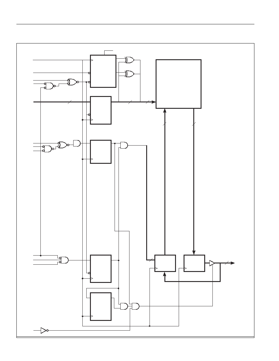
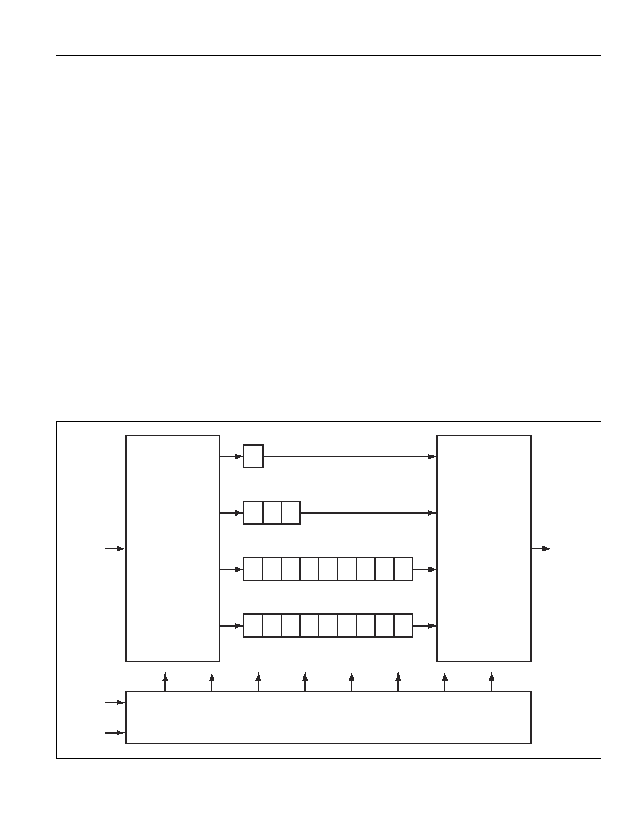
BLOCK DIAGRAM
18/19
BINARY
COUNTER
GW
CLR
CE
CLK
Q0
Q1
MODE
A0'
A0
A1
A1'
CLK
ADV
ADSC
ADSP
16/17
18/19
ADDRESS
REGISTER
CE
D
CLK
Q
DQ(a-d)
BYTE WRITE
REGISTERS
D
CLK
Q
ENABLE
REGISTER
CE
D
CLK
Q
ENABLE
DELAY
REGISTER
D
CLK
Q
BWE
BW(a-d)
x18: a,b
x36: a-d
CE
CE2
CE2
256Kx36;
512Kx18
MEMORY ARRAY
36,
or 18
INPUT
REGISTERS
CLK
OUTPUT
REGISTERS
CLK
OE
2/4/8
OE
DQa - DQd
36,
or 18
36,
or 18
A
Integrated Silicon Solution, Inc. -- 1-800-379-4774
3
Rev. A
05/09/05
IS61VPD25636A, IS61VPD51218A, IS61LPD25636A, IS61LPD51218A
ISSI
Æ
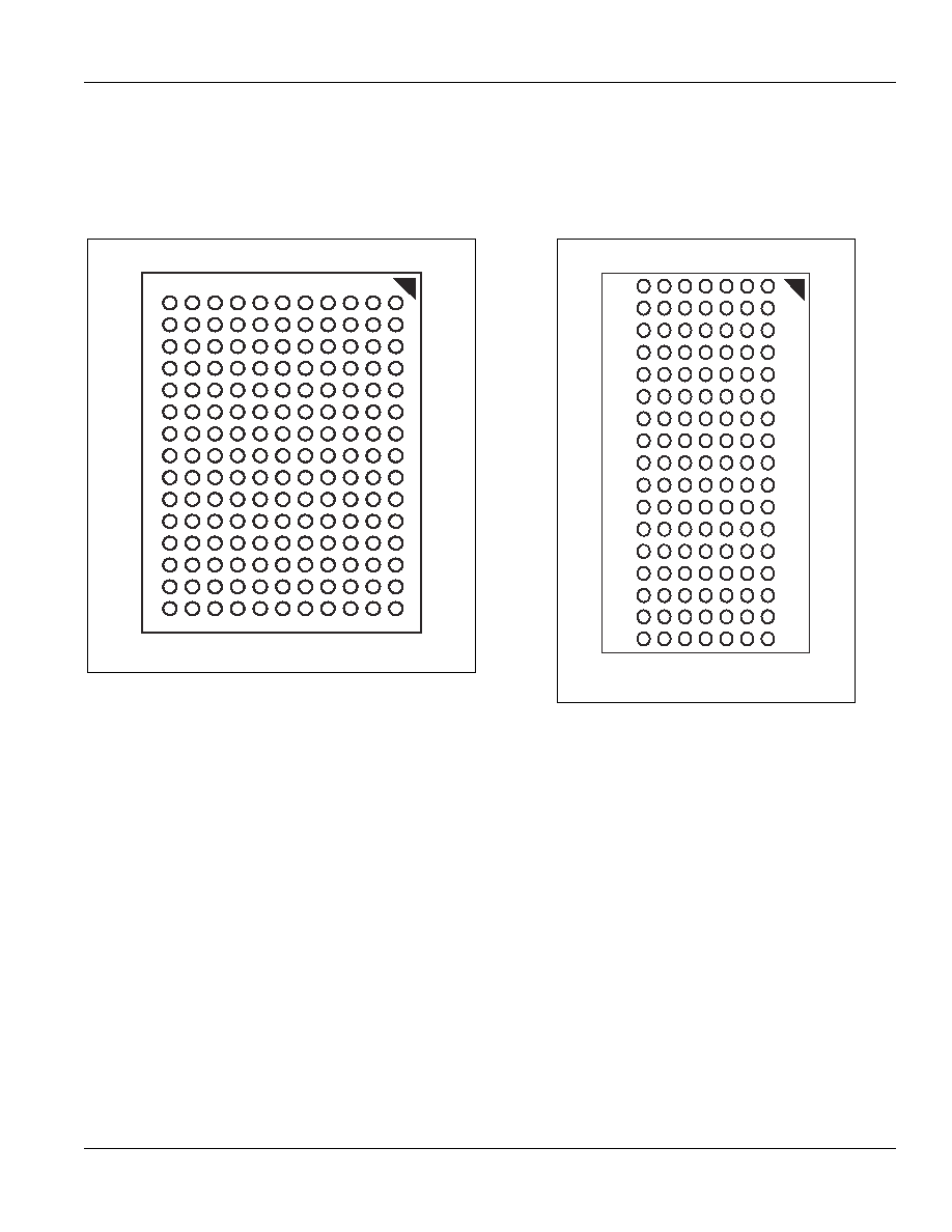
BOTTOM VIEW
BOTTOM VIEW
165-PIN BGA
165-Ball, 13x15 mm BGA
1mm Ball Pitch, 11x15 Ball Array
119-PIN BGA
119-Ball, 14x22 mm BGA
1mm Ball Pitch, 7x17 Ball Array

4
Integrated Silicon Solution, Inc. -- 1-800-379-4774
Rev. A
05/09/05
IS61VPD25636A, IS61VPD51218A, IS61LPD25636A, IS61LPD51218A
ISSI
Æ
119 BGA PACKAGE PIN CONFIGURATION-
256K
X
36
(TOP VIEW)
PIN DESCRIPTIONS
1
2
3
4
5
6
7
A
V
DDQ
A
A
ADSP
A
A
V
DDQ
B
NC
CE2
A
ADSC
A
A
NC
C
NC
A
A
V
DD
A
A
NC
D
DQc
DQPc
Vss
NC
Vss
DQPb
DQb
E
DQc
DQc
Vss
CE
Vss
DQb
DQb
F
V
DDQ
DQc
Vss
OE
Vss
DQb
V
DDQ
G
DQc
DQc
BWc
ADV
BWb
DQb
DQb
H
DQc
DQc
Vss
GW
Vss
DQb
DQb
J
V
DDQ
V
DD
NC
V
DD
NC
V
DD
V
DDQ
K
DQd
DQd
Vss
CLK
Vss
DQa
DQa
L
DQd
DQd
BWd
NC
BWa
DQa
DQa
M
V
DDQ
DQd
Vss
BWE
Vss
DQa
V
DDQ
N
DQd
DQd
Vss
A
1
*
Vss
DQa
DQa
P
DQd
DQPd
Vss
A
0
*
Vss
DQPa
DQa
R
NC
A
MODE
V
DD
NC
A
NC
T
NC
NC
A
A
A
NC
ZZ
U
V
DDQ
TMS
TDI
TCK
TDO
NC
V
DDQ
Symbol
Pin Name
A
Address Inputs
A0, A1
Synchronous Burst Address Inputs
ADV
Synchronous Burst Address
Advance
ADSP
Address Status Processor
ADSC
Address Status Controller
GW
Global Write Enable
CLK
Synchronous Clock
CE
, CE2
Synchronous Chip Select
BW
x (x=a-d)
Synchronous Byte Write Controls
BWE
Byte Write Enable
Symbol
Pin Name
OE
Output Enable
ZZ
Power Sleep Mode
MODE
Burst Sequence Selection
TCK, TDO
JTAG Pins
TMS, TDI
NC
No Connect
DQa-DQd
Data Inputs/Outputs
DQPa-Pd
Output Power Supply
V
DD
Power Supply
V
DDQ
Output Power Supply
Vss
Ground
Note: * A
0
and A
1
are the two least significant bits (LSB) of the address field and set the internal burst counter if burst is desired.

Integrated Silicon Solution, Inc. -- 1-800-379-4774
5
Rev. A
05/09/05
IS61VPD25636A, IS61VPD51218A, IS61LPD25636A, IS61LPD51218A
ISSI
Æ
119 BGA PACKAGE PIN CONFIGURATION
512K
X
18
(TOP VIEW)
PIN DESCRIPTIONS
Note: * A
0
and A
1
are the two least significant bits (LSB) of the address field and set the internal burst counter if burst is
desired.
1
2
3
4
5
6
7
A
V
DDQ
A
A
ADSP
A
A
V
DDQ
B
NC
CE2
A
ADSC
A
A
NC
C
NC
A
A
V
DD
A
A
NC
D
DQb
NC
Vss
NC
Vss
DQPa
NC
E
NC
DQb
Vss
CE
Vss
NC
DQa
F
V
DDQ
NC
Vss
OE
Vss
DQa
V
DDQ
G
NC
DQb
BWb
ADV
Vss
NC
DQa
H
DQb
NC
Vss
GW
Vss
DQa
NC
J
V
DDQ
V
DD
NC
V
DD
NC
V
DD
V
DDQ
K
NC
DQb
Vss
CLK
Vss
NC
DQa
L
DQb
NC
Vss
NC
BWa
DQa
NC
M
V
DDQ
DQb
Vss
BWE
Vss
NC
V
DDQ
N
DQb
NC
Vss
A
1
*
Vss
DQa
NC
P
NC
DQPb
Vss
A
0
*
Vss
NC
DQa
R
NC
A
MODE
V
DD
NC
A
NC
T
NC
A
A
NC
A
A
ZZ
U
V
DDQ
TMS
TDI
TCK
TDO
NC
V
DDQ
Symbol
Pin Name
A
Address Inputs
A0, A1
Synchronous Burst Address Inputs
ADV
Synchronous Burst Address
Advance
ADSP
Address Status Processor
ADSC
Address Status Controller
GW
Global Write Enable
CLK
Synchronous Clock
CE
, CE2
Synchronous Chip Select
BW
x (x=a,b)
Synchronous Byte Write Controls
BWE
Byte Write Enable
Symbol
Pin Name
OE
Output Enable
ZZ
Power Sleep Mode
MODE
Burst Sequence Selection
TCK, TDO
JTAG Pins
TMS, TDI
NC
No Connect
DQa-DQb
Data Inputs/Outputs
DQPa-Pb
Output Power Supply
V
DD
Power Supply
V
DDQ
Output Power Supply
Vss
Ground

6
Integrated Silicon Solution, Inc. -- 1-800-379-4774
Rev. A
05/09/05
IS61VPD25636A, IS61VPD51218A, IS61LPD25636A, IS61LPD51218A
ISSI
Æ
PIN DESCRIPTIONS
165 PBGA PACKAGE PIN CONFIGURATION
256K
X
36 (TOP VIEW)
Note: * A
0
and A
1
are the two least significant bits (LSB) of the address field and set the internal burst counter if burst is
desired.
1
2
3
4
5
6
7
8
9
10
11
A
NC
A
CE
BWc
BWb
CE2
BWE
ADSC
ADV
A
NC
B
NC
A
CE2
BWd
BWa
CLK
GW
OE
ADSP
A
NC
C
DQPc
NC
V
DDQ
Vss
Vss
Vss
Vss
Vss
V
DDQ
NC
DQPb
D
DQc
DQc
V
DDQ
V
DD
Vss
Vss
Vss
V
DD
V
DDQ
DQb
DQb
E
DQc
DQc
V
DDQ
V
DD
Vss
Vss
Vss
V
DD
V
DDQ
DQb
DQb
F
DQc
DQc
V
DDQ
V
DD
Vss
Vss
Vss
V
DD
V
DDQ
DQb
DQb
G
DQc
DQc
V
DDQ
V
DD
Vss
Vss
Vss
V
DD
V
DDQ
DQb
DQb
H
NC
Vss
NC
V
DD
Vss
Vss
Vss
V
DD
NC
NC
ZZ
J
DQd
DQd
V
DDQ
V
DD
Vss
Vss
Vss
V
DD
V
DDQ
DQa
DQa
K
DQd
DQd
V
DDQ
V
DD
Vss
Vss
Vss
V
DD
V
DDQ
DQa
DQa
L
DQd
DQd
V
DDQ
V
DD
Vss
Vss
Vss
V
DD
V
DDQ
DQa
DQa
M
DQd
DQd
V
DDQ
V
DD
Vss
Vss
Vss
V
DD
V
DDQ
DQa
DQa
N
DQPd
NC
V
DDQ
Vss
NC
NC
NC
Vss
V
DDQ
NC DQPa
P
NC
NC
A
A
TDI
A
1
*
TDO
A
A
A
A
R
MODE
NC
A
A
TMS
A
0
*
TCK
A
A
A
A
Symbol
Pin Name
A
Address Inputs
A0, A1
Synchronous Burst Address Inputs
ADV
Synchronous Burst Address
Advance
ADSP
Address Status Processor
ADSC
Address Status Controller
GW
Global Write Enable
CLK
Synchronous Clock
CE
,
CE2
,
CE2
Synchronous Chip Select
BW
x (x=a,b,c,d) Synchronous Byte Write
Controls
Symbol
Pin Name
BWE
Byte Write Enable
OE
Output Enable
ZZ
Power Sleep Mode
MODE
Burst Sequence Selection
TCK, TDO
JTAG Pins
TMS, TDI
NC
No Connect
DQx
Data Inputs/Outputs
DQPx
Data Inputs/Outputs
V
DD
3.3V/2.5V Power Supply
V
DDQ
Isolated Output Power Supply
3.3V
/2.5V
Vss
Ground
Integrated Silicon Solution, Inc. -- 1-800-379-4774
7
Rev. A
05/09/05
IS61VPD25636A, IS61VPD51218A, IS61LPD25636A, IS61LPD51218A
ISSI
Æ
Note: * A
0
and A
1
are the two least significant bits (LSB) of the address field and set the internal burst counter if burst is
desired.
165 PBGA PACKAGE PIN CONFIGURATION
512K
X
18 (TOP VIEW)
PIN DESCRIPTIONS
1
2
3
4
5
6
7
8
9
10
11
A
NC
A
CE
BWb
NC
CE2
BWE
ADSC
ADV
A
A
B
NC
A
CE2
NC
BWa
CLK
GW
OE
ADSP
A
NC
C
NC
NC
V
DDQ
Vss
Vss
Vss
Vss
Vss
V
DDQ
NC
DQPa
D
NC
DQb
V
DDQ
V
DD
Vss
Vss
Vss
V
DD
V
DDQ
NC
DQa
E
NC
DQb
V
DDQ
V
DD
Vss
Vss
Vss
V
DD
V
DDQ
NC
DQa
F
NC
DQb
V
DDQ
V
DD
Vss
Vss
Vss
V
DD
V
DDQ
NC
DQa
G
NC
DQb
V
DDQ
V
DD
Vss
Vss
Vss
V
DD
V
DDQ
NC
DQa
H
NC
Vss
NC
V
DD
Vss
Vss
Vss
V
DD
NC
NC
ZZ
J
DQb
NC
V
DDQ
V
DD
Vss
Vss
Vss
V
DD
V
DDQ
DQa
NC
K
DQb
NC
V
DDQ
V
DD
Vss
Vss
Vss
V
DD
V
DDQ
DQa
NC
L
DQb
NC
V
DDQ
V
DD
Vss
Vss
Vss
V
DD
V
DDQ
DQa
NC
M
DQb
NC
V
DDQ
V
DD
Vss
Vss
Vss
V
DD
V
DDQ
DQa
NC
N
DQPb
NC
V
DDQ
Vss
NC
NC
NC
Vss
V
DDQ
NC
NC
P
NC
NC
A
A
TDI
A
1
*
TDO
A
A
A
A
R
MODE
NC
A
A
TMS
A
0
*
TCK
A
A
A
A
Symbol
Pin Name
A
Address Inputs
A0, A1
Synchronous Burst Address Inputs
ADV
Synchronous Burst Address
Advance
ADSP
Address Status Processor
ADSC
Address Status Controller
GW
Global Write Enable
CLK
Synchronous Clock
CE
,
CE2
,
CE2
Synchronous Chip Select
BW
x (x=a,b)
Synchronous Byte Write
Controls
Symbol
Pin Name
BWE
Byte Write Enable
OE
Output Enable
ZZ
Power Sleep Mode
MODE
Burst Sequence Selection
TCK, TDO
JTAG Pins
TMS, TDI
NC
No Connect
DQx
Data Inputs/Outputs
DQPx
Data Inputs/Outputs
V
DD
3.3V/2.5V Power Supply
V
DDQ
Isolated Output Power Supply
3.3V/2.5V
Vss
Ground

8
Integrated Silicon Solution, Inc. -- 1-800-379-4774
Rev. A
05/09/05
IS61VPD25636A, IS61VPD51218A, IS61LPD25636A, IS61LPD51218A
ISSI
Æ
DQPb
DQb
DQb
VDDQ
VSS
DQb
DQb
DQb
DQb
VSS
VDDQ
DQb
DQb
VSS
NC
VDD
ZZ
DQa
DQa
VDDQ
VSS
DQa
DQa
DQa
DQa
VSS
VDDQ
DQa
DQa
DQPa
A
A
CE
CE2
BWd
BWc
BWb
BWa
CE2
VDD
VSS
CLK
GW
BWE
OE
ADSC
ADSP
ADV
A
A
DQPc
DQc
DQc
VDDQ
VSS
DQc
DQc
DQc
DQc
VSS
VDDQ
DQc
DQc
NC
VDD
NC
VSS
DQd
DQd
VDDQ
VSS
DQd
DQd
DQd
DQd
VSS
VDDQ
DQd
DQd
DQPd
1
2
3
4
5
6
7
8
9
10
11
12
13
14
15
16
17
18
19
20
21
22
23
24
25
26
27
28
29
30
80
79
78
77
76
75
74
73
72
71
70
69
68
67
66
65
64
63
62
61
60
59
58
57
56
55
54
53
52
51
100 99 98 97 96 95 94 93 92 91 90 89 88 87 86 85 84 83 82 81
31 32 33 34 35 36 37 38 39 40 41 42 43 44 45
MODE
A
A
A
A
A1
A0
NC
NC
VSS
VDD
NC
A
A
A
A
A
A
A
A
46 47 48 49 50
PIN DESCRIPTIONS
A0, A1
Synchronous Address Inputs. These
pins must tied to the two LSBs of the
address bus.
A
Synchronous Address Inputs
ADSC
Synchronous Controller Address
Status
ADSP
Synchronous Processor Address
Status
ADV
Synchronous Burst Address Advance
BWa
-
BWd
Synchronous Byte Write Enable
BWE
Synchronous Byte Write Enable
CE
,
CE2
,
CE2 Synchronous Chip Enable
CLK
Synchronous Clock
DQa-DQd
Synchronous Data Input/Output
DQPa-DQPd
Parity Data Input/Output
GW
Synchronous Global Write Enable
MODE
Burst Sequence Mode Selection
OE
Output Enable
V
DD
3.3V/2.5V Power Supply
V
DDQ
Isolated Output Buffer Supply:
3.3V/2.5V
Vss
Ground
ZZ
Snooze Enable
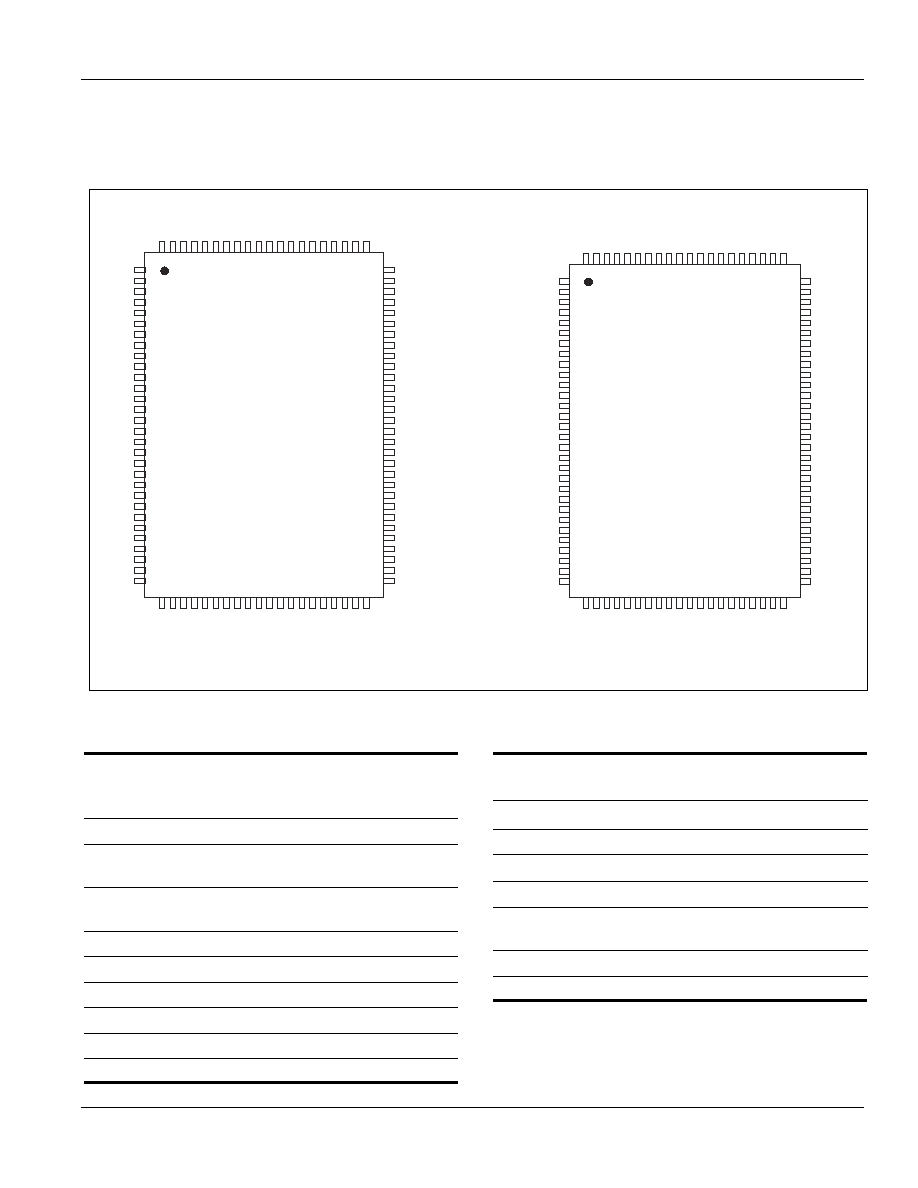
PIN CONFIGURATION
(3 Chip-Enable option)
100-PIN TQFP (256K X 36)
DQPb
DQb
DQb
VDDQ
VSS
DQb
DQb
DQb
DQb
VSS
VDDQ
DQb
DQb
VSS
NC
VDD
ZZ
DQa
DQa
VDDQ
VSS
DQa
DQa
DQa
DQa
VSS
VDDQ
DQa
DQa
DQPa
A
A
CE
CE2
BWd
BWc
BWb
BWa
A
V
DD
VSS
CLK
GW
BWE
OE
ADS
C
ADSP
ADV
A
A
DQPc
DQc
DQc
VDDQ
VSS
DQc
DQc
DQc
DQc
VSS
VDDQ
DQc
DQc
NC
VDD
NC
VSS
DQd
DQd
VDDQ
VSS
DQd
DQd
DQd
DQd
VSS
VDDQ
DQd
DQd
DQPd
1
2
3
4
5
6
7
8
9
10
11
12
13
14
15
16
17
18
19
20
21
22
23
24
25
26
27
28
29
30
80
79
78
77
76
75
74
73
72
71
70
69
68
67
66
65
64
63
62
61
60
59
58
57
56
55
54
53
52
51
100 99 98 97 96 95 94 93 92 91 90 89 88 87 86 85 84 83 82 81
31 32 33 34 35 36 37 38 39 40 41 42 43 44 45
MODE
A
A
A
A
A1
A0
NC
NC
VSS
V
DD
NC
NC
A
A
A
A
A
A
A
46 47 48 49 50
(2 Chip-Enable option)
Integrated Silicon Solution, Inc. -- 1-800-379-4774
9
Rev. A
05/09/05
IS61VPD25636A, IS61VPD51218A, IS61LPD25636A, IS61LPD51218A
ISSI
Æ
PIN CONFIGURATION
(3 Chip-Enable Option)
PIN DESCRIPTIONS
A0, A1
Synchronous Address Inputs. These
pins must tied to the two LSBs of the
address bus.
A
Synchronous Address Inputs
ADSC
Synchronous Controller Address
Status
ADSP
Synchronous Processor Address
Status
ADV
Synchronous Burst Address Advance
BWa
-
BWb
Synchronous Byte Write Enable
BWE
Synchronous Byte Write Enable
CE
, CE2,
CE2
Synchronous Chip Enable
CLK
Synchronous Clock
DQa-DQb
Synchronous Data Input/Output
DQPa-DQPb
Parity Data I/O; DQPa is parity for
DQa1-8; DQPb is parity for DQb1-8
GW
Synchronous Global Write Enable
MODE
Burst Sequence Mode Selection
OE
Output Enable
V
DD
3.3V/2.5V Power Supply
V
DDQ
Isolated Output Buffer Supply:
3.3V/2.5V
Vss
Ground
ZZ
Snooze Enable
100-PIN TQFP (512K X 18)
A
NC
NC
VDDQ
VSS
NC
DQPa
DQa
DQa
VSS
VDDQ
DQa
DQa
VSS
NC
VDD
ZZ
DQa
DQa
VDDQ
VSS
DQa
DQa
NC
NC
VSS
VDDQ
NC
NC
NC
A
A
CE
CE2
NC
NC
BWb
BWa
CE2
VDD
VSS
CLK
GW
BWE
OE
ADSC
ADSP
ADV
A
A
NC
NC
NC
VDDQ
VSS
NC
NC
DQb
DQb
VSS
VDDQ
DQb
DQb
NC
VDD
NC
VSS
DQb
DQb
VDDQ
VSS
DQb
DQb
DQPb
NC
VSS
VDDQ
NC
NC
NC
1
2
3
4
5
6
7
8
9
10
11
12
13
14
15
16
17
18
19
20
21
22
23
24
25
26
27
28
29
30
80
79
78
77
76
75
74
73
72
71
70
69
68
67
66
65
64
63
62
61
60
59
58
57
56
55
54
53
52
51
100 99 98 97 96 95 94 93 92 91 90 89 88 87 86 85 84 83 82 81
31 32 33 34 35 36 37 38 39 40 41 42 43 44 45
MODE
A
A
A
A
A1
A0
NC
NC
VSS
VDD
NC
A
A
A
A
A
A
A
A
46 47 48 49 50
(2 Chip-Enable Option)
A
NC
NC
V
DDQ
VSS
NC
DQPa
DQa
DQa
VSS
V
DDQ
DQa
DQa
VSS
NC
V
DD
ZZ
DQa
DQa
V
DDQ
VSS
DQa
DQa
NC
NC
VSS
V
DDQ
NC
NC
NC
A
A
CE
CE2
NC
NC
BWb
BWa
A
V
DD
VSS
CLK
GW
BWE
OE
ADSC
ADSP
ADV
A
A
NC
NC
NC
V
DDQ
VSS
NC
NC
DQb
DQb
VSS
V
DDQ
DQb
DQb
NC
V
DD
NC
VSS
DQb
DQb
V
DDQ
VSS
DQb
DQb
DQPb
NC
VSS
V
DDQ
NC
NC
NC
1
2
3
4
5
6
7
8
9
10
11
12
13
14
15
16
17
18
19
20
21
22
23
24
25
26
27
28
29
30
80
79
78
77
76
75
74
73
72
71
70
69
68
67
66
65
64
63
62
61
60
59
58
57
56
55
54
53
52
51
100 99 98 97 96 95 94 93 92 91 90 89 88 87 86 85 84 83 82 81
31 32 33 34 35 36 37 38 39 40 41 42 43 44 45
MODE
A
A
A
A
A1
A0
NC
NC
VSS
V
DD
NC
NC
A
A
A
A
A
A
A
46 47 48 49 50

10
Integrated Silicon Solution, Inc. -- 1-800-379-4774
Rev. A
05/09/05
IS61VPD25636A, IS61VPD51218A, IS61LPD25636A, IS61LPD51218A
ISSI
Æ
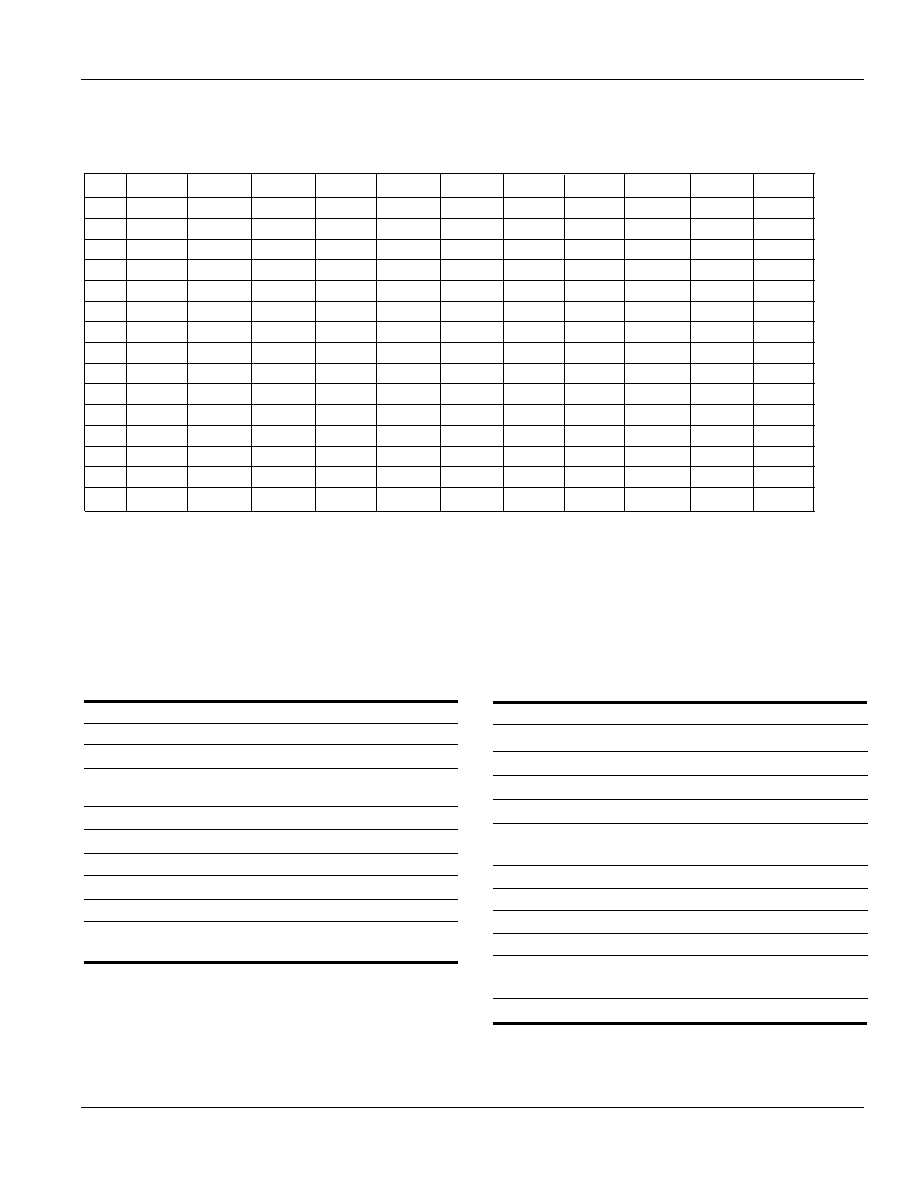
PARTIAL TRUTH TABLE
Function
GW
GW
GW
GW
GW
BWE
BWE
BWE
BWE
BWE
BWa
BWa
BWa
BWa
BWa
BWb
BWb
BWb
BWb
BWb
BWc
BWc
BWc
BWc
BWc
BWd
BWd
BWd
BWd
BWd
Read
H
H
X
X
X
X
Read
H
L
H
H
H
H
Write Byte 1
H
L
L
H
H
H
Write All Bytes
H
L
L
L
L
L
Write All Bytes
L
X
X
X
X
X
TRUTH TABLE
(1-8)
OPERATION
ADDRESS
CE
CE
CE
CE
CE
CE2
CE2
CE2
CE2
CE2
CE2
ZZ
ADSP
ADSP
ADSP
ADSP
ADSP ADSC
ADSC
ADSC
ADSC
ADSC ADV
ADV
ADV
ADV
ADV
WRITE
WRITE
WRITE
WRITE
WRITE OE
OE
OE
OE
OE
CLK
DQ
Deselect Cycle, Power-Down
None
H
X
X
L
X
L
X
X
X
L-H
High-Z
Deselect Cycle, Power-Down
None
L
X
L
L
L
X
X
X
X
L-H
High-Z
Deselect Cycle, Power-Down
None
L
H
X
L
L
X
X
X
X
L-H
High-Z
Deselect Cycle, Power-Down
None
L
X
L
L
H
L
X
X
X
L-H
High-Z
Deselect Cycle, Power-Down
None
L
H
X
L
H
L
X
X
X
L-H
High-Z
Snooze Mode, Power-Down
None
X
X
X
H
X
X
X
X
X
X
High-Z
Read Cycle, Begin Burst
External
L
L
H
L
L
X
X
X
L
L-H
Q
Read Cycle, Begin Burst
External
L
L
H
L
L
X
X
X
H
L-H
High-Z
Write Cycle, Begin Burst
External
L
L
H
L
H
L
X
L
X
L-H
D
Read Cycle, Begin Burst
External
L
L
H
L
H
L
X
H
L
L-H
Q
Read Cycle, Begin Burst
External
L
L
H
L
H
L
X
H
H
L-H
High-Z
Read Cycle, Continue Burst
Next
X
X
X
L
H
H
L
H
L
L-H
Q
Read Cycle, Continue Burst
Next
X
X
X
L
H
H
L
H
H
L-H
High-Z
Read Cycle, Continue Burst
Next
H
X
X
L
X
H
L
H
L
L-H
Q
Read Cycle, Continue Burst
Next
H
X
X
L
X
H
L
H
H
L-H
High-Z
Write Cycle, Continue Burst
Next
X
X
X
L
H
H
L
L
X
L-H
D
Write Cycle, Continue Burst
Next
H
X
X
L
X
H
L
L
X
L-H
D
Read Cycle, Suspend Burst
Current
X
X
X
L
H
H
H
H
L
L-H
Q
Read Cycle, Suspend Burst
Current
X
X
X
L
H
H
H
H
H
L-H
High-Z
Read Cycle, Suspend Burst
Current
H
X
X
L
X
H
H
H
L
L-H
Q
Read Cycle, Suspend Burst
Current
H
X
X
L
X
H
H
H
H
L-H
High-Z
Write Cycle, Suspend Burst
Current
X
X
X
L
H
H
H
L
X
L-H
D
Write Cycle, Suspend Burst
Current
H
X
X
L
X
H
H
L
X
L-H
D
NOTE:
1. X means "Don't Care." H means logic HIGH. L means logic LOW.
2. For
WRITE
, L means one or more byte write enable signals (
BWa-d
) and
BWE
are LOW or
GW
is LOW.
WRITE
= H for all
BWx
,
BWE
,
GW
HIGH.
3.
BWa
enables WRITEs to DQa's and DQPa.
BWb
enables WRITEs to DQb's and DQPb.
BWc
enables WRITEs to DQc's and
DQPc.
BWd
enables WRITEs to DQd's and DQPd. DQPa and DQPb are available on the x18 version. DQPa-DQPd are
available on the x36 version.
4. All inputs except
OE
and ZZ must meet setup and hold times around the rising edge (LOW to HIGH) of CLK.
5. Wait states are inserted by suspending burst.
6. For a WRITE operation following a READ operation,
OE
must be HIGH before the input data setup time and held HIGH during
the input data hold time.
7. This device contains circuitry that will ensure the outputs will be in High-Z during power-up.
8.
ADSP
LOW always initiates an internal READ at the L-H edge of CLK. A WRITE is performed by setting one or more byte
write enable signals and
BWE
LOW or
GW
LOW for the subsequent L-H edge of CLK. See WRITE timing diagram for
clarification.
Integrated Silicon Solution, Inc. -- 1-800-379-4774
11
Rev. A
05/09/05
IS61VPD25636A, IS61VPD51218A, IS61LPD25636A, IS61LPD51218A
ISSI
Æ
INTERLEAVED BURST ADDRESS TABLE (MODE = V
DD
or No Connect)
External Address
1st Burst Address
2nd Burst Address
3rd Burst Address
A1 A0
A1 A0
A1 A0
A1 A0
00
01
10
11
01
00
11
10
10
11
00
01
11
10
01
00
LINEAR BURST ADDRESS TABLE (MODE = VSS)
0,0
1,0
0,1
A1', A0' = 1,1
ABSOLUTE MAXIMUM RATINGS
(1)
Symbol
Parameter
Value
Unit
T
STG
Storage Temperature
≠55 to +150
∞C
P
D
Power Dissipation
1.6
W
I
OUT
Output Current (per I/O)
100
mA
V
IN
, V
OUT
Voltage Relative to Vss for I/O Pins
≠0.5 to V
DDQ
+ 0.5
V
V
IN
Voltage Relative to Vss for
≠0.5 to V
DD
+ 0.5
V
for Address and Control Inputs
V
DD
Voltage on V
DD
Supply Relative to Vss
≠0.5 to 4.6
V
Notes:
1. Stress greater than those listed under ABSOLUTE MAXIMUM RATINGS may cause perma-
nent damage to the device. This is a stress rating only and functional operation of the device at
these or any other conditions above those indicated in the operational sections of this
specification is not implied. Exposure to absolute maximum rating conditions for extended
periods may affect reliability.
2. This device contains circuity to protect the inputs against damage due to high static voltages or
electric fields; however, precautions may be taken to avoid application of any voltage higher than
maximum rated voltages to this high-impedance circuit.
3. This device contains circuitry that will ensure the output devices are in High-Z at power up.

12
Integrated Silicon Solution, Inc. -- 1-800-379-4774
Rev. A
05/09/05
IS61VPD25636A, IS61VPD51218A, IS61LPD25636A, IS61LPD51218A
ISSI
Æ
OPERATING RANGE (IS61LPDXXXXX)
Range
Ambient Temperature
V
DD
V
DDQ
Commercial
0∞C to +70∞C
3.3V + 5%
3.3 / 2.5V + 5%
Industrial
≠40∞C to +85∞C
3.3V + 5%
3.3 / 2.5V + 5%
OPERATING RANGE (IS61VPDXXXXX)
Range
Ambient Temperature
V
DD
V
DDQ
Commercial
0∞C to +70∞C
2.5V + 5%
2.5V + 5%
Industrial
≠40∞C to +85∞C
2.5V + 5%
2.5V + 5%
DC ELECTRICAL CHARACTERISTICS
(Over Operating Range)
3.3V
2.5V
Symbol
Parameter
Test Conditions
Min.
Max.
Min.
Max.
Unit
V
OH
Output HIGH Voltage
I
OH
= ≠4.0 mA (3.3V)
2.4
--
2.0
--
V
I
OH
= ≠1.0 mA (2.5V)
V
OL
Output LOW Voltage
I
OL
= 8.0 mA (3.3V)
--
0.4
--
0.4
V
I
OL
= 1.0 mA (2.5V)
V
IH
Input HIGH Voltage
2.0
V
DD
+ 0.3
1.7
V
DD
+ 0.3
V
V
IL
Input LOW Voltage
-0.3
0.8
-0.3
0.7
V
I
LI
Input Leakage Current
Vss
V
IN
V
DD
(1)
-5
5
-5
5
µA
I
LO
Output Leakage Current Vss
V
OUT
V
DDQ
,
-5
5
-5
5
µA
OE
= V
IH
POWER SUPPLY CHARACTERISTICS
(1)
(Over Operating Range)
-250
-200
MAX
MAX
Symbol Parameter
Test Conditions
Temp. range
x18
x36
x18
x36
Unit
I
CC
AC Operating
Device Selected,
Com.
275
275
250
250
mA
Supply Current
OE
= V
IH
, ZZ
V
IL
,
I
ND
.
300
300
275
275
All Inputs
0.2V or
V
DD
≠ 0.2V,
Cycle Time
t
KC
min.
I
SB
Standby Current
Device Deselected,
C
OM
.
150
150
150
150
mA
TTL Input
V
DD
= Max.,
Ind.
150
150
150
150
All Inputs
V
IL
or
V
IH
,
ZZ
V
IL
, f = Max.
I
SBI
Standby Current
Device Deselected,
Com.
100
100
100
100
mA
CMOS Input
V
DD
= Max.,
Ind.
105
105
105
105
V
IN
V
SS
+ 0.2V or
V
DD
≠ 0.2V
f = 0
I
SB
2
Sleep Mode
ZZ>V
IH
Com.
50
50
50
50
mA
Ind.
60
60
60
60
Note:
1. MODE pin has an internal pullup and should be tied to V
DD
or V
SS
. It exhibits ±100µA maximum leakage current when tied to
V
SS
+ 0.2V or
V
DD
≠ 0.2V.
Integrated Silicon Solution, Inc. -- 1-800-379-4774
13
Rev. A
05/09/05
IS61VPD25636A, IS61VPD51218A, IS61LPD25636A, IS61LPD51218A
ISSI
Æ
CAPACITANCE
(1,2)
Symbol
Parameter
Conditions
Max.
Unit
C
IN
Input Capacitance
V
IN
= 0V
6
pF
C
OUT
Input/Output Capacitance
V
OUT
= 0V
8
pF
Notes:
1. Tested initially and after any design or process changes that may affect these parameters.
2. Test conditions: T
A
= 25∞C, f = 1 MHz, V
DD
= 3.3V.
3.3V I/O AC TEST CONDITIONS
Parameter
Unit
Input Pulse Level
0V to 3.0V
Input Rise and Fall Times
1.5 ns
Input and Output Timing
1.5V
and Reference Level
Output Load
See Figures 1 and 2
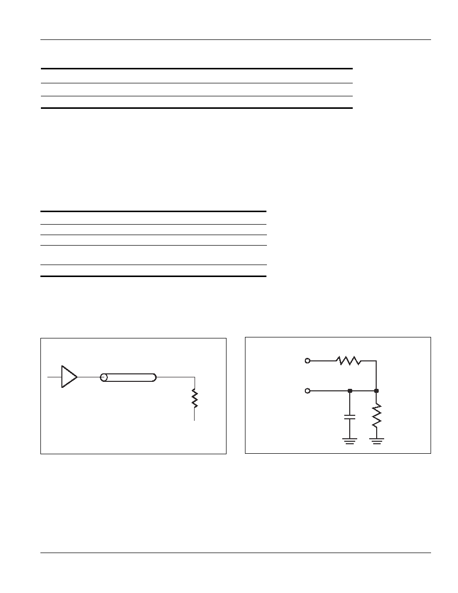
AC TEST LOADS
Figure 2
317
5 pF
Including
jig and
scope
351
OUTPUT
3.3V
Figure 1
Output
Buffer
Z
O
= 50
1.5V
50
14
Integrated Silicon Solution, Inc. -- 1-800-379-4774
Rev. A
05/09/05
IS61VPD25636A, IS61VPD51218A, IS61LPD25636A, IS61LPD51218A
ISSI
Æ
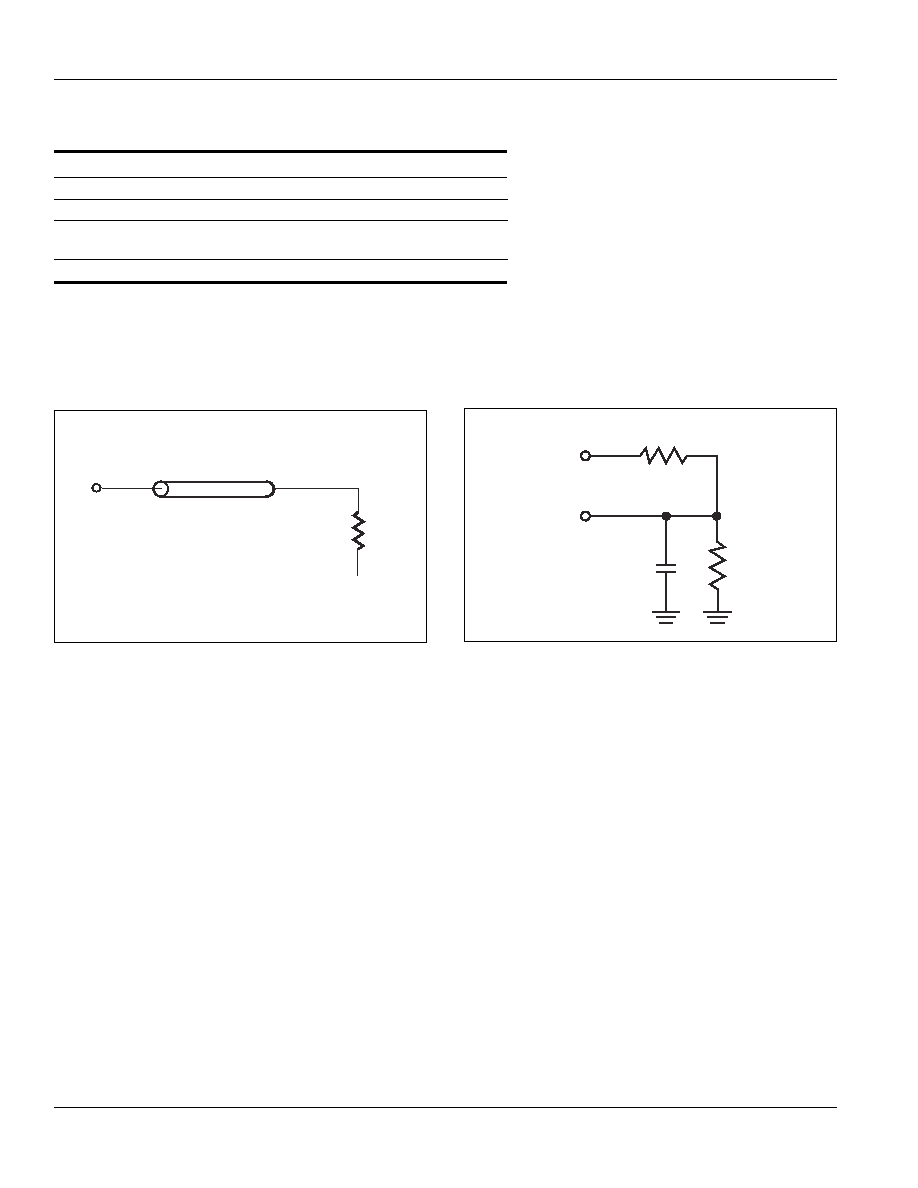
2.5V I/O AC TEST CONDITIONS
Parameter
Unit
Input Pulse Level
0V to 2.5V
Input Rise and Fall Times
1.5 ns
Input and Output Timing
1.25V
and Reference Level
Output Load
See Figures 3 and 4
2.5 I/O OUTPUT LOAD EQUIVALENT
Figure 4
1,667
5 pF
Including
jig and
scope
1,538
OUTPUT
2.5V
Figure 3
Output
Z
O
= 50
1.25V
50

Integrated Silicon Solution, Inc. -- 1-800-379-4774
15
Rev. A
05/09/05
IS61VPD25636A, IS61VPD51218A, IS61LPD25636A, IS61LPD51218A
ISSI
Æ
READ/WRITE CYCLE SWITCHING CHARACTERISTICS
(Over Operating Range)
-250
-200
Symbol
Parameter
Min.
Max.
Min.
Max.
Unit
f
MAX
Clock Frequency
--
250
--
200
MHz
t
KC
Cycle Time
4.0
--
5
--
ns
t
KH
Clock High Time
1.7
--
2
--
ns
t
KL
Clock Low Time
1.7
--
2
--
ns
t
KQ
Clock Access Time
--
2.6
--
3.1
ns
t
KQX
(2)
Clock High to Output Invalid
0.8
--
1.5
--
ns
t
KQLZ
(2,3)
Clock High to Output Low-Z
0.8
--
1
--
ns
t
KQHZ
(2,3)
Clock High to Output High-Z
--
2.6
--
3.0
ns
t
OEQ
Output Enable to Output Valid
--
2.6
--
3.1
ns
t
OELZ
(2,3)
Output Enable to Output Low-Z
0
--
0
--
ns
t
OEHZ
(2,3)
Output Disable to Output High-Z
--
2.6
--
3.0
ns
t
AS
Address Setup Time
1.2
--
1.4
--
ns
t
WS
Read/Write Setup Time
1.2
--
1.4
--
ns
t
CES
Chip Enable Setup Time
1.2
--
1.4
--
ns
t
AVS
Address Advance Setup Time
1.2
--
1.4
--
ns
t
DS
Data Setup Time
1.2
--
1.4
--
ns
t
AH
Address Hold Time
0.3
--
0.4
--
ns
t
WH
Write Hold Time
0.3
--
0.4
--
ns
t
CEH
Chip Enable Hold Time
0.3
--
0.4
--
ns
t
AVH
Address Advance Hold Time
0.3
--
0.4
--
ns
t
DH
Data Hold Time
0.3
--
0.4
--
ns
t
PDS
ZZ High to Power Down
--
2
--
2
cyc
t
PUS
ZZ Low to Power Down
--
2
--
2
cyc
Note:
1. Configuration signal MODE is static and must not change during normal operation.
2. Guaranteed but not 100% tested. This parameter is periodically sampled.
3. Tested with load in Figure 2.

16
Integrated Silicon Solution, Inc. -- 1-800-379-4774
Rev. A
05/09/05
IS61VPD25636A, IS61VPD51218A, IS61LPD25636A, IS61LPD51218A
ISSI
Æ
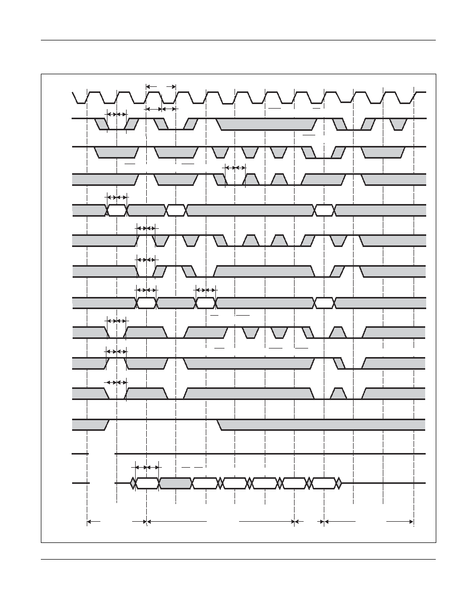
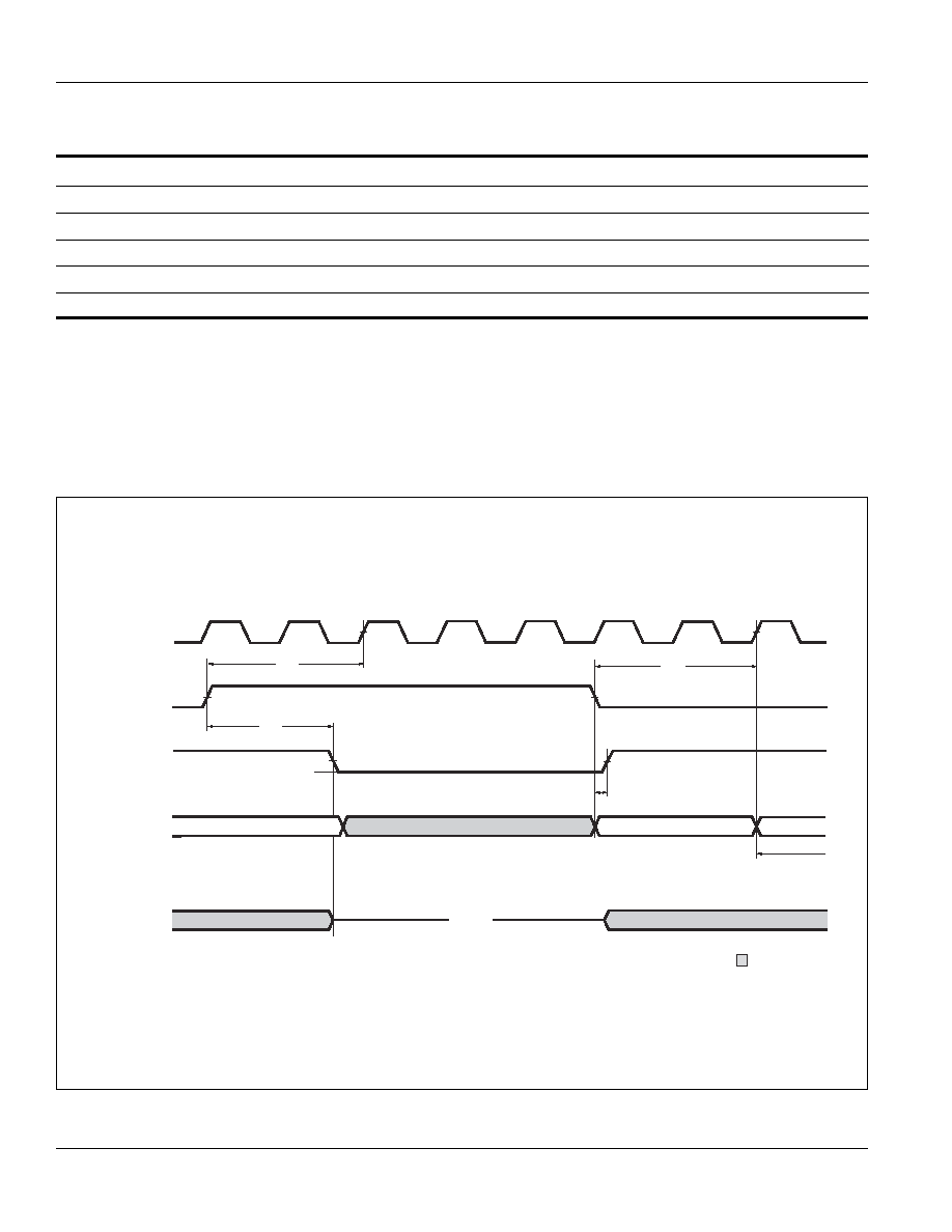
READ/WRITE CYCLE TIMING
Single Read
High-Z
High-Z
DATA
OUT
DATA
IN
OE
CE2
CE2
CE
BWx
BWE
GW
Address
ADV
ADSC
ADSP
CLK
RD1
RD2
1a
2c
2d
3a
Unselected
Burst Read
t
KQX
t
KC
t
KL
t
KH
t
SS
t
SH
t
SS
t
SH
t
AS
t
AH
t
WS
t
WH
t
WS
t
WH
RD3
t
CES
t
CEH
t
CES
t
CEH
t
CES
t
CEH
CE2 and CE2 only sampled with ADSP or ADSC
CE Masks ADSP
Unselected with CE2
t
OEQ
t
OEQX
t
OELZ
t
KQLZ
t
KQ
t
OEHZ
t
KQHZ
ADSC initiate read
ADSP is blocked by CE inactive
t
AVH
t
AVS
Suspend Burst
Pipelined Read
2a
2b
Integrated Silicon Solution, Inc. -- 1-800-379-4774
17
Rev. A
05/09/05
IS61VPD25636A, IS61VPD51218A, IS61LPD25636A, IS61LPD51218A
ISSI
Æ
WRITE CYCLE TIMING
Single Write
DATA
OUT
DATA
IN
OE
CE2
CE2
CE
BWx
BWE
GW
Address
ADV
ADSC
ADSP
CLK
WR1
WR2
Unselected
Burst Write
t
KC
t
KL
t
KH
t
SS
t
SH
t
AS
t
AH
t
WS
t
WH
t
WS
t
WH
WR3
t
CES
t
CEH
t
CES
t
CEH
t
CES
t
CEH
CE2 and CE2 only sampled with ADSP or ADSC
CE Masks ADSP
Unselected with CE2
ADSC initiate Write
ADSP is blocked by CE inactive
t
AVH
t
AVS
ADV must be inactive for ADSP Write
WR1
WR2
t
WS
t
WH
WR3
t
WS
t
WH
High-Z
High-Z
1a
3a
t
DS
t
DH
BW4-BW1 only are applied to first cycle of WR2
Write
2c
2d
2a
2b
18
Integrated Silicon Solution, Inc. -- 1-800-379-4774
Rev. A
05/09/05
IS61VPD25636A, IS61VPD51218A, IS61LPD25636A, IS61LPD51218A
ISSI
Æ
SNOOZE MODE TIMING
Don't Care
Deselect or Read Only
Deselect or Read Only
t
RZZI
CLK
ZZ
Isupply
All Inputs
(except ZZ)
Outputs
(Q)
I
SB2
ZZ setup cycle
ZZ recovery cycle
Normal
operation
cycle
t
PDS
t
PUS
t
ZZI
High-Z
SNOOZE MODE ELECTRICAL CHARACTERISTICS
Symbol
Parameter
Conditions
Min.
Max.
Unit
I
SB
2
Current during SNOOZE MODE
ZZ
Vih
--
60
mA
t
PDS
ZZ active to input ignored
--
2
cycle
t
PUS
ZZ inactive to input sampled
2
--
cycle
t
ZZI
ZZ active to SNOOZE current
--
2
cycle
t
RZZI
ZZ inactive to exit SNOOZE current
0
--
ns
Integrated Silicon Solution, Inc. -- 1-800-379-4774
19
Rev. A
05/09/05
IS61VPD25636A, IS61VPD51218A, IS61LPD25636A, IS61LPD51218A
ISSI
Æ
IEEE 1149.1 SERIAL BOUNDARY SCAN (JTAG)
The IS61LPD/VPD25636A and IS61LPD/VPD51218A have
a serial boundary scan Test Access Port (TAP) in the PBGA
package only. (The TQFP package not available.) This port
operates in accordance with IEEE Standard 1149.1-1900,
but does not include all functions required for full 1149.1
compliance. These functions from the IEEE specification are
excluded because they place added delay in the critical
speed path of the SRAM. The TAP controller operates in a
manner that does not conflict with the performance of other
devices using 1149.1 fully compliant TAPs. The TAP
operates using JEDEC standard 2.5V I/O logic levels.
DISABLING THE JTAG FEATURE
The SRAM can operate without using the JTAG feature. To
disable the TAP controller, TCK must be tied LOW (Vss) to
prevent clocking of the device. TDI and TMS are internally
pulled up and may be disconnected. They may alternately
be connected to V
DD
through a pull-up resistor. TDO should
be left disconnected. On power-up, the device will start in a
reset state which will not interfere with the device operation.
TEST ACCESS PORT (TAP) - TEST CLOCK
The test clock is only used with the TAP controller. All
inputs are captured on the rising edge of TCK and outputs
are driven from the falling edge of TCK.
TEST MODE SELECT (TMS)
The TMS input is used to send commands to the TAP
controller and is sampled on the rising edge of TCK. This
pin may be left disconnected if the TAP is not used. The
pin is internally pulled up, resulting in a logic HIGH level.
TEST DATA-IN (TDI)
The TDI pin is used to serially input information to the
registers and can be connected to the input of any
register. The register between TDI and TDO is chosen by
the instruction loaded into the TAP instruction register.
For information on instruction register loading, see the
TAP Controller State Diagram. TDI is internally pulled up
and can be disconnected if the TAP is unused in an
application. TDI is connected to the Most Significant Bit
(MSB) on any register.
31 30 29
. . .
2 1 0
2 1 0
0
x
. . . . .
2 1 0
Bypass Register
Instruction Register
Identification Register
Boundary Scan Register*
TAP CONTROLLER
Selection Circuitry
Selection Circuitry
TDO
TDI
TCK
TMS
TAP CONTROLLER BLOCK DIAGRAM

20
Integrated Silicon Solution, Inc. -- 1-800-379-4774
Rev. A
05/09/05
IS61VPD25636A, IS61VPD51218A, IS61LPD25636A, IS61LPD51218A
ISSI
Æ
TEST DATA OUT (TDO)
The TDO output pin is used to serially clock data-out from
the registers. The output is active depending on the current
state of the TAP state machine (see TAP Controller State
Diagram). The output changes on the falling edge of TCK
and TDO is connected to the Least Significant Bit (LSB) of
any register.
PERFORMING A TAP RESET
A Reset is performed by forcing TMS HIGH (V
DD
) for five
rising edges of TCK. RESET may be performed while the
SRAM is operating and does not affect its operation. At
power-up, the TAP is internally reset to ensure that TDO
comes up in a high-Z state.
TAP REGISTERS
Registers are connected between the TDI and TDO pins
and allow data to be scanned into and out of the SRAM test
circuitry. Only one register can be selected at a time
through the instruction registers. Data is serially loaded
into the TDI pin on the rising edge of TCK and output on the
TDO pin on the falling edge of TCK.
Instruction Register
Three-bit instructions can be serially loaded into the
instruction register. This register is loaded when it is
placed between the TDI and TDO pins. (See TAP Controller
Block Diagram) At power-up, the instruction register is
loaded with the IDCODE instruction. It is also loaded with
the IDCODE instruction if the controller is placed in a reset
state as previously described.
When the TAP controller is in the CaptureIR state, the two
least significant bits are loaded with a binary "01" pattern
to allow for fault isolation of the board level serial test path.
Bypass Register
To save time when serially shifting data through registers,
it is sometimes advantageous to skip certain states. The
bypass register is a single-bit register that can be placed
between TDI and TDO pins. This allows data to be shifted
through the SRAM with minimal delay. The bypass register
is set LOW (Vss) when the BYPASS instruction is ex-
ecuted.
Boundary Scan Register
The boundary scan register is connected to all input and
output pins on the SRAM. Several no connect (NC) pins are
also included in the scan register to reserve pins for higher
density devices. The x36 configuration has a 75-bit-long
register and the x18 configuration also has a 75-bit-long
register. The boundary scan register is loaded with the
contents of the RAM Input and Output ring when the TAP
controller is in the Capture-DR state and then placed
between the TDI and TDO pins when the controller is moved
to the Shift-DR state. The EXTEST, SAMPLE/PRELOAD
and SAMPLE-Z instructions can be used to capture the
contents of the Input and Output ring.
The Boundary Scan Order tables show the order in which the
bits are connected. Each bit corresponds to one of the
bumps on the SRAM package. The MSB of the register is
connected to TDI, and the LSB is connected to TDO.
Identification (ID) Register
The ID register is loaded with a vendor-specific, 32-bit
code during the Capture-DR state when the IDCODE
command is loaded to the instruction register. The IDCODE
is hardwired into the SRAM and can be shifted out when
the TAP controller is in the Shift-DR state. The ID register
has vendor code and other information described in the
Identification Register Definitions table.
Scan Register Sizes
Register Name
Bit Size (x18)
Bit Size (x36)
Instruction
3
3
Bypass
1
1
ID
32
32
Boundary Scan
75
75
IDENTIFICATION REGISTER DEFINITIONS
Instruction Field
Description
256K x 36
512K x 18
Revision Number (31:28)
Reserved for version number.
xxxx
xxxx
Device Depth (27:23)
Defines depth of SRAM. 256K or 512K
00111
01000
Device Width (22:18)
Defines with of the SRAM. x36 or x18
00100
00011
ISSI Device ID (17:12)
Reserved for future use.
xxxxx
xxxxx
ISSI JEDEC ID (11:1)
Allows unique identification of SRAM vendor.
00011010101
00011010101
ID Register Presence (0)
Indicate the presence of an ID register.
1
1

Integrated Silicon Solution, Inc. -- 1-800-379-4774
21
Rev. A
05/09/05
IS61VPD25636A, IS61VPD51218A, IS61LPD25636A, IS61LPD51218A
ISSI
Æ
TAP INSTRUCTION SET
Eight instructions are possible with the three-bit instruction
register and all combinations are listed in the Instruction
Code table. Three instructions are listed as RESERVED
and should not be used and the other five instructions are
described below. The TAP controller used in this SRAM is
not fully compliant with the 1149.1 convention because
some mandatory instructions are not fully implemented.
The TAP controller cannot be used to load address, data or
control signals and cannot preload the Input or Output
buffers. The SRAM does not implement the 1149.1 com-
mands EXTEST or INTEST or the PRELOAD portion of
SAMPLE/PRELOAD; instead it performs a capture of the
Inputs and Output ring when these instructions are executed.
Instructions are loaded into the TAP controller during the
Shift-IR state when the instruction register is placed
between TDI and TDO. During this state, instructions are
shifted from the instruction register through the TDI and
TDO pins. To execute an instruction once it is shifted in,
the TAP controller must be moved into the Update-IR
state.
EXTEST
EXTEST is a mandatory 1149.1 instruction which is to be
executed whenever the instruction register is loaded with
all 0s. Because EXTEST is not implemented in the TAP
controller, this device is not 1149.1 standard compliant.
The TAP controller recognizes an all-0 instruction. When
an EXTEST instruction is loaded into the instruction
register, the SRAM responds as if a SAMPLE/PRELOAD
instruction has been loaded. There is a difference between
the instructions, unlike the SAMPLE/PRELOAD instruction,
EXTEST places the SRAM outputs in a High-Z state.
IDCODE
The IDCODE instruction causes a vendor-specific, 32-bit
code to be loaded into the instruction register. It also
places the instruction register between the TDI and TDO
pins and allows the IDCODE to be shifted out of the device
when the TAP controller enters the Shift-DR state. The
IDCODE instruction is loaded into the instruction register
upon power-up or whenever the TAP controller is given a
test logic reset state.
SAMPLE-Z
The SAMPLE-Z instruction causes the boundary scan
register to be connected between the TDI and TDO pins
when the TAP controller is in a Shift-DR state. It also
places all SRAM outputs into a High-Z state.
SAMPLE/PRELOAD
SAMPLE/PRELOAD is a 1149.1 mandatory instruction.
The PRELOAD portion of this instruction is not imple-
mented, so the TAP controller is not fully 1149.1 compli-
ant. When the SAMPLE/PRELOAD instruction is loaded
to the instruction register and the TAP controller is in the
Capture-DR state, a snapshot of data on the inputs and
output pins is captured in the boundary scan register.
It is important to realize that the TAP controller clock
operates at a frequency up to 10 MHz, while the SRAM
clock runs more than an order of magnitude faster.
Because of the clock frequency differences, it is possible
that during the Capture-DR state, an input or output will
under-go a transition. The TAP may attempt a signal
capture while in transition (metastable state). The device
will not be harmed, but there is no guarantee of the value
that will be captured or repeatable results.
To guarantee that the boundary scan register will capture
the correct signal value, the SRAM signal must be
stabilized long enough to meet the TAP controller's
capture set-up plus hold times (t
CS
and t
CH
). To insure that
the SRAM clock input is captured correctly, designs need
a way to stop (or slow) the clock during a SAMPLE/
PRELOAD instruction. If this is not an issue, it is possible
to capture all other signals and simply ignore the value of
the CLK and
CLK
captured in the boundary scan register.
Once the data is captured, it is possible to shift out the data
by putting the TAP into the Shift-DR state. This places the
boundary scan register between the TDI and TDO pins.
Note that since the PRELOAD part of the command is not
implemented, putting the TAP into the Update to the Update-DR
state while performing a SAMPLE/PRELOAD instruction
will have the same effect as the Pause-DR command.
BYPASS
When the BYPASS instruction is loaded in the instruction
register and the TAP is placed in a Shift-DR state, the
bypass register is placed between the TDI and TDO pins.
The advantage of the BYPASS instruction is that it
shortens the boundary scan path when multiple devices
are connected together on a board.
RESERVED
These instructions are not implemented but are reserved
for future use. Do not use these instructions.
22
Integrated Silicon Solution, Inc. -- 1-800-379-4774
Rev. A
05/09/05
IS61VPD25636A, IS61VPD51218A, IS61LPD25636A, IS61LPD51218A
ISSI
Æ
INSTRUCTION CODES
Code
Instruction
Description
000
EXTEST
Captures the Input/Output ring contents. Places the boundary scan register
between the TDI and TDO. Forces all SRAM outputs to High-Z state. This
instruction is not 1149.1 compliant.
001
IDCODE
Loads the ID register with the vendor ID code and places the register between
TDI and TDO. This operation does not affect SRAM operation.
010
SAMPLE-Z
Captures the Input/Output contents. Places the boundary scan register between TDI
and TDO. Forces all SRAM output drivers to a High-Z state.
011
RESERVED
Do Not Use: This instruction is reserved for future use.
100
SAMPLE/PRELOAD
Captures the Input/Output ring contents. Places the boundary scan register between
TDI and TDO. Does not affect the SRAM operation. This instruction does not
implement 1149.1 preload function and is therefore not 1149.1 compliant.
101
RESERVED
Do Not Use: This instruction is reserved for future use.
110
RESERVED
Do Not Use: This instruction is reserved for future use.
111
BYPASS
Places the bypass register between TDI and TDO. This operation does not
affect SRAM operation.
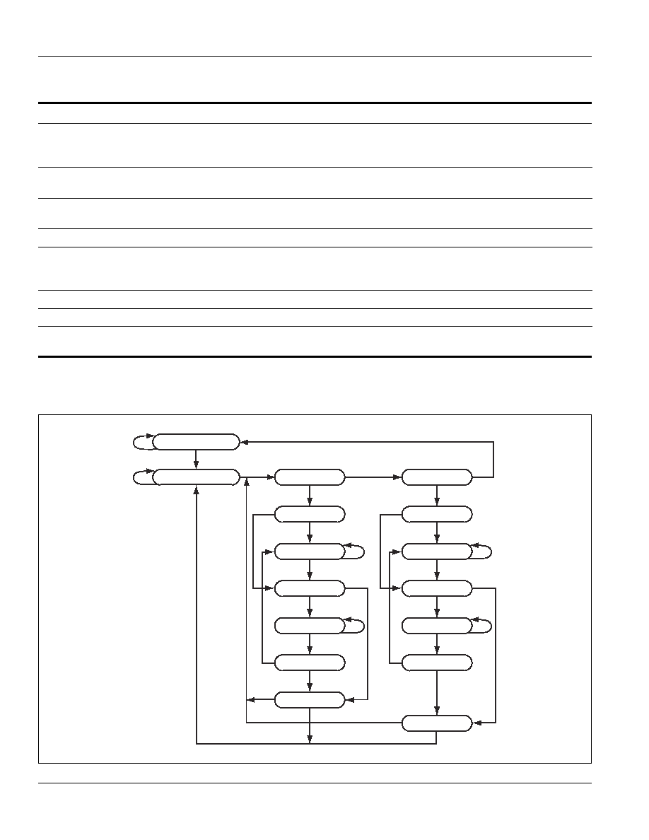
Select DR
Capture DR
Shift DR
Exit1 DR
Pause DR
Exit2 DR
Update DR
Select IR
Capture IR
Shift IR
Exit1 IR
Pause IR
Exit2 IR
Update IR
Test Logic Reset
Run Test/Idle
1
1
1
1
1
1
1
1
1
1
1
1
1
1
0
0
0
0
1
0
0
0
0
0
0
0
0
0
0
0
1
0
TAP CONTROLLER STATE DIAGRAM

Integrated Silicon Solution, Inc. -- 1-800-379-4774
23
Rev. A
05/09/05
IS61VPD25636A, IS61VPD51218A, IS61LPD25636A, IS61LPD51218A
ISSI
Æ
TAP Electrical Characteristics Over the Operating Range
(1,2)
Symbol
Parameter
Test Conditions
Min.
Max.
Units
V
OH1
Output HIGH Voltage
I
OH
= ≠2.0 mA
1.7
--
V
V
OH2
Output HIGH Voltage
I
OH
= ≠100 µA
2.1
--
V
V
OL1
Output LOW Voltage
I
OL
= 2.0 mA
--
0.7
V
V
OL2
Output LOW Voltage
I
OL
= 100 µA
--
0.2
V
V
IH
Input HIGH Voltage
1.7
V
DD
+0.3
V
V
IL
Input LOW Voltage
≠0.3
0.7
V
I
X
Input Load Current
Vss
V I
V
DDQ
≠5
5
mA
Notes:
1. All Voltage referenced to Ground.
2. Overshoot: V
IH
(AC)
V
DD
+1.5V for t
t
TCYC
/2,
Undershoot:V
IL
(AC)
0.5V for t
t
TCYC
/2,
Power-up: V
IH
< 2.6V and V
DD
< 2.4V and V
DDQ
< 1.4V for t < 200 ms.
TAP AC ELECTRICAL CHARACTERISTICS
(1,2)
(OVER OPERATING RANGE)
Symbol Parameter
Min.
Max.
Unit
t
TCYC
TCK Clock cycle time
100
--
ns
f
TF
TCK Clock frequency
--
10
MHz
t
TH
TCK Clock HIGH
40
--
ns
t
TL
TCK Clock LOW
40
--
ns
t
TMSS
TMS setup to TCK Clock Rise
10
--
ns
t
TDIS
TDI setup to TCK Clock Rise
10
--
ns
t
CS
Capture setup to TCK Rise
10
--
ns
t
TMSH
TMS hold after TCK Clock Rise
10
--
ns
t
TDIH
TDI Hold after Clock Rise
10
--
ns
t
CH
Capture hold after Clock Rise
10
--
ns
t
TDOV
TCK LOW to TDO valid
--
20
ns
t
TDOX
TCK LOW to TDO invalid
0
--
ns
Notes:
1. Both t
CS
and t
CH
refer to the set-up and hold time latching data requirements from the boundary scan register.
2. Test conditions are specified using the load in TAP AC test conditions. t
R
/t
F
= 1 ns.

24
Integrated Silicon Solution, Inc. -- 1-800-379-4774
Rev. A
05/09/05
IS61VPD25636A, IS61VPD51218A, IS61LPD25636A, IS61LPD51218A
ISSI
Æ
DON'T CARE
UNDEFINED
TCK
TMS
TDI
TDO
t
THTL
t
TLTH
t
THTH
t
MVTH
t
THMX
t
DVTH
t
THDX
1 2 3 4 5 6
t
TLOX
t
TLOV
TAP TIMING
20 pF
TDO
GND
50
1.25V
Z
0
= 50
TAP Output Load Equivalent
TAP AC TEST CONDITIONS (2.5/3.3V)
Input pulse levels
0 to 2.5V/0 to 3.0V
Input rise and fall times
1ns
Input timing reference levels
1.25V/1.5V
Output reference levels
1.25V/1.5V
Test load termination supply voltage
1.25V/1.5V

Integrated Silicon Solution, Inc. -- 1-800-379-4774
25
Rev. A
05/09/05
IS61VPD25636A, IS61VPD51218A, IS61LPD25636A, IS61LPD51218A
ISSI
Æ
119 BGA BOUNDARY SCAN ORDER (256K X 36)
Signal Bump
Signal Bump
Signal Bump
Signal Bump
Bit #
Name
ID
Bit #
Name
ID
Bit #
Name
ID
Bit #
Name
ID
1
A
2R
19
DQb
7G
37
BWa
5L
55
DQd
2K
2
A
3T
20
DQb
6F
38
BWb
5G
56
DQd
1L
3
A
4T
21
DQb
7E
39
BWc
3G
57
DQd
2M
4
A
5T
22
DQb
7D
40
BWd
3L
58
DQd
1N
5
A
6R
23
DQb
7H
41
CE2
2B
59
DQd
1P
6
A
3B
24
DQb
6G
42
CE
4E
60
DQd
1K
7
A
5B
25
DQb
6E
43
A
3A
61
DQd
2L
8
DQa
6P
26
DQb
6D
44
A
2A
62
DQd
2N
9
DQa
7N
27
A
6A
45
DQc
2D
63
DQd
2P
10
DQa
6M
28
A
5A
46
DQc
1E
64
MODE
3R
11
DQa
7L
29
ADV
4G
47
DQc
2F
65
A
2C
12
DQa
6K
30
ADSP
4A
48
DQc
1G
66
A
3C
13
DQa
7P
31
ADSC
4B
49
DQc
2H
67
A
5C
14
DQa
6N
32
OE
4F
50
DQc
1D
68
A
6C
15
DQa
6L
33
BWE
4M
51
DQc
2E
69
A1
4N
16
DQa
7K
34
GW
4H
52
DQc
2G
70
A0
4P
17
ZZ
7T
35
CLK
4K
53
DQc
1H
18
DQb
6H
36
A
6B
54
NC
5R
119 BGA BOUNDARY SCAN ORDER (512K X 18)
Signal Bump
Signal Bump
Signal Bump
Signal Bump
Bit #
Name
ID
Bit #
Name
ID
Bit #
Name
ID
Bit #
Name
ID
1
A
2R
14
DQa
7G
27
CLK
4K
40
DQb
2K
2
A
2T
15
DQa
6F
28
A
6B
41
DQb
1L
3
A
3T
16
DQa
7E
29
BWa
5L
42
DQb
2M
4
A
5T
17
DQa
6D
30
BWb
3G
43
DQb
1N
5
A
6R
18
A
6T
31
CE2
2B
44
DQb
2P
6
A
3B
19
A
6A
32
CE
4E
45
MODE
3R
7
A
5B
20
A
5A
33
A
3A
46
A
2C
8
DQa
7P
21
ADV
4G
34
A
2A
47
A
3C
9
DQa
6N
22
ADSP
4A
35
DQb
1D
48
A
5C
10
DQa
6L
23
ADSC
4B
36
DQb
2E
49
A
6C
11
DQa
7K
24
OE
4F
37
DQb
2G
50
A1
4N
12
ZZ
7T
25
BWE
4M
38
DQb
1H
51
A0
4P
13
DQa
6H
26
GW
4H
39
NC
5R

26
Integrated Silicon Solution, Inc. -- 1-800-379-4774
Rev. A
05/09/05
IS61VPD25636A, IS61VPD51218A, IS61LPD25636A, IS61LPD51218A
ISSI
Æ
165 PBGA BOUNDARY SCAN ORDER (x 36)
Signal Bump
Signal
Bump
Signal
Bump
Signal
Bump
Bit #
Name
ID
Bit #
Name
ID
Bit #
Name
ID
Bit #
Name
ID
1
MODE
1R
21
DQb
11G
41
NC
1A
61
DQd
1J
2
NC
6N
22
DQb
11F
42
CE
2
6A
62
DQd
1K
3
A
11P
23
DQb
11E
43
BW
a
5B
63
DQd
1L
4
A
8P
24
DQb
11D
44
BW
b
5A
64
DQd
1M
5
A
8R
25
DQb
10G
45
BW
c
4A
65
DQd
2J
6
A
9R
26
DQb
10F
46
BW
d
4B
66
DQd
2K
7
A
9P
27
DQb
10E
47
CE2
3B
67
DQd
2L
8
A
10P
28
DQb
10D
48
CE
3A
68
DQd
2M
9
A
10R
29
DQb
11C
49
A
2A
69
DQd
1N
10
A
11R
30
NC
11A
50
A
2B
70
A
3P
11
ZZ
11H
31
A
10A
51
NC
1B
71
A
3R
12
DQa
11N
32
A
10B
52
DQc
1C
72
A
4R
13
DQa
11M
33
ADV
9A
53
DQc
1D
73
A
4P
14
DQa
11L
34
ADSP
9B
54
DQc
1E
74
A1
6P
15
DQa
11K
35
ADSC
8A
55
DQc
1F
75
A0
6R
16
DQa
11J
36
OE
8B
56
DQc
1G
17
DQa
10M
37
BWE
7A
57
DQc
2D
18
DQa
10L
38
GW
7B
58
DQc
2E
19
DQa
10K
39
CLK
6B
59
DQc
2F
20
DQa
10J
40
NC
11B
60
DQc
2G

Integrated Silicon Solution, Inc. -- 1-800-379-4774
27
Rev. A
05/09/05
IS61VPD25636A, IS61VPD51218A, IS61LPD25636A, IS61LPD51218A
ISSI
Æ
165 PBGA BOUNDARY SCAN ORDER (x 18)
Signal Bump
Signal
Bump
Signal
Bump
Signal
Bump
Bit #
Name
ID
Bit #
Name
ID
Bit #
Name
ID
Bit #
Name
ID
1
MODE
1R
21
DQa
11G
41
NC
1A
61
DQb
1J
2
NC
6N
22
DQa
11F
42
CE
2
6A
62
DQb
1K
3
A
11P
23
DQa
11E
43
BW
a
5B
63
DQb
1L
4
A
8P
24
DQa
11D
44
NC
5A
64
DQb
1M
5
A
8R
25
DQa
11C
45
BW
b
4A
65
DQb
1N
6
A
9R
26
NC
10F
46
NC
4B
66
NC
2K
7
A
9P
27
NC
10E
47
CE2
3B
67
NC
2L
8
A
10P
28
NC
10D
48
CE
3A
68
NC
2M
9
A
10R
29
NC
10G
49
A
2A
69
NC
2J
10
A
11R
30
A
11A
50
A
2B
70
A
3P
11
ZZ
11H
31
A
10A
51
NC
1B
71
A
3R
12
NC
11N
32
A
10B
52
NC
1C
72
A
4R
13
NC
11M
33
ADV
9A
53
NC
1D
73
A
4P
14
NC
11L
34
ADSP
9B
54
NC
1E
74
A1
6P
15
NC
11K
35
ADSC
8A
55
NC
1F
75
A0
6R
16
NC
11J
36
OE
8B
56
NC
1G
17
DQa
10M
37
BWE
7A
57
DQb
2D
18
DQa
10L
38
GW
7B
58
DQb
2E
19
DQa
10K
39
CLK
6B
59
DQb
2F
20
DQa
10J
40
NC
11B
60
DQb
2G

28
Integrated Silicon Solution, Inc. -- 1-800-379-4774
Rev. A
05/09/05
IS61VPD25636A, IS61VPD51218A, IS61LPD25636A, IS61LPD51218A
ISSI
Æ
ORDERING INFORMATION (3.3V core/2.5V-3.3V I/O)
Commercial Range: 0∞C to +70∞C
Configuration
Frequency
Order Part Number
Package
(1)
256Kx36
250
IS61LPD25636A-250TQ
100 TQFP, 3CE
IS61LPD25636A-250B2
119 PBGA
IS61LPD25636A-250B3
165 PBGA
200
IS61LPD25636A-200TQ
100 TQFP, 3CE
IS61LPD25636A-200B2
119 PBGA
IS61LPD25636A-200B3
165 PBGA
512Kx18
250
IS61LPD51218A-250TQ
100 TQFP, 3CE
IS61LPD51218A-250B2
119 PBGA
IS61LPD51218A-250B3
165 PBGA
200
IS61LPD51218A-200TQ
100 TQFP, 3CE
IS61LPD51218A-200B2
119 PBGA
IS61LPD51218A-200B3
165 PBGA
Industrial Range: -40∞C to +85∞C
Configuration
Frequency
Order Part Number
Package
(1)
256Kx36
250
IS61LPD25636A-250TQI
100 TQFP, 3CE
IS61LPD25636A-250B2I
119 PBGA
IS61LPD25636A-250B3I
165 PBGA
200
IS61LPD25636A-200TQI
100 TQFP, 3CE
IS61LPD25636A-200TQ2I
100 TQFP, 2CE
IS61LPD25636A-200B2I
119 PBGA
IS61LPD25636A-200B3I
165 PBGA
512Kx18
250
IS61LPD51218A-250TQI
100 TQFP, 3CE
IS61LPD51218A-250B2I
119 PBGA
IS61LPD51218A-250B3I
165 PBGA
200
IS61LPD51218A-200TQI
100 TQFP, 3CE
IS61LPD51218A-200B2I
119 PBGA
IS61LPD51218A-200B3I
165 PBGA
Note:
1. For 100 TQFP, 2CE option contact SRAM Marketing at sram@issi.com

Integrated Silicon Solution, Inc. -- 1-800-379-4774
29
Rev. A
05/09/05
IS61VPD25636A, IS61VPD51218A, IS61LPD25636A, IS61LPD51218A
ISSI
Æ
ORDERING INFORMATION (2.5V core/2.5V I/O)
Commercial Range: 0∞C to +70∞C
Configuration
Frequency
Order Part Number
Package
(1)
256Kx36
250
IS61VPD25636A-250TQ
100 TQFP, 3CE
IS61VPD25636A-250B2
119 PBGA
IS61VPD25636A-250B3
165 PBGA
200
IS61VPD25636A-200TQ
100 TQFP, 3CE
IS61VPD25636A-200B2
119 PBGA
IS61VPD25636A-200B3
165 PBGA
512Kx18
250
IS61VPD51218A-250TQ
100 TQFP, 3CE
IS61VPD51218A-250B2
119 PBGA
IS61VPD51218A-250B3
165 PBGA
200
IS61VPD51218A-200TQ
100 TQFP, 3CE
IS61VPD51218A-200B2
119 PBGA
IS61VPD51218A-200B3
165 PBGA
Industrial Range: -40∞C to +85∞C
Configuration
Frequency
Order Part Number
Package
(1)
256Kx36
250
IS61VPD25636A-250TQI
100 TQFP, 3CE
IS61VPD25636A-250B2I
119 PBGA
IS61VPD25636A-250B3I
165 PBGA
200
IS61VPD25636A-200TQI
100 TQFP, 3CE
IS61VPD25636A-200TQ2I
100 TQFP, 2CE
IS61VPD25636A-200B2I
119 PBGA
IS61VPD25636A-200B3I
165 PBGA
512Kx18
250
IS61VPD51218A-250TQI
100 TQFP, 3CE
IS61VPD51218A-250B2I
119 PBGA
IS61VPD51218A-250B3I
165 PBGA
200
IS61VPD51218A-200TQI
100 TQFP, 3CE
IS61VPD51218A-200B2I
119 PBGA
IS61VPD51218A-200B3I
165 PBGA
Note:
1. For 100 TQFP, 2CE option contact SRAM Marketing at sram@issi.com
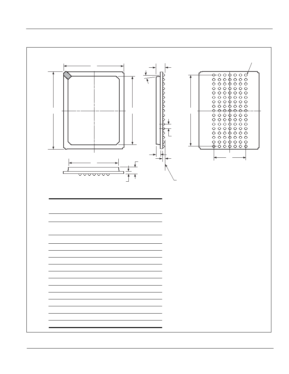
PACKAGING INFORMATION
ISSI
Æ
Integrated Silicon Solution, Inc. -- www.issi.com --
1-800-379-4774
Rev. B
02/12/03
Copyright © 2003 Integrated Silicon Solution, Inc. All rights reserved. ISSI reserves the right to make changes to this specification and its products at any time
without notice. ISSI assumes no liability arising out of the application or use of any information, products or services described herein. Customers are advised to
obtain the latest version of this device specification before relying on any published information and before placing orders for products.
Plastic Ball Grid Array
Package Code: B (119-pin)
Notes:
1. Controlling dimension: millimeters, unless otherwise specified.
2. BSC = Basic lead spacing between centers.
3. Dimensions D1 and E do not include mold flash protrusion and
should be measured from the bottom of the package.
4. Formed leads shall be planar with respect to one another within
0.004 inches at the seating plane.
MILLIMETERS
INCHES
Sym.
Min.
Max.
Min.
Max.
N0.
Leads
119
A
--
2.41
--
0.095
A1
0.50
0.70
0.020
0.028
A2
0.80
1.00
0.032
0.039
A3
1.30
1.70
0.051
0.067
A4
0.56 BSC
0.022 BSC
b
0.60
0.90
0.024
0.035
D
21.80
22.20
0.858
0.874
D1
20.32 BSC
0.800 BSC
D2
19.40
19.60
0.764
0.772
E
13.80
14.20
0.543
0.559
E1
7.62 BSC
0.300 BSC
E2
11.90
12.10
0.469
0.476
e
1.27 BSC
0.050 BSC
E1
A1
D1
7
6
5
4
3
2
1
A
B
C
D
E
F
G
H
J
K
L
M
N
P
R
T
U
E2
E
A2
SEATING PLANE
e
D2
D
A
30
A3
A4
b (119X)
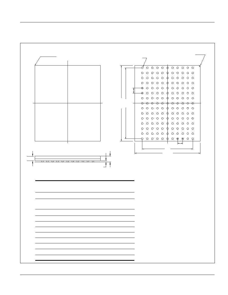
PACKAGING INFORMATION
ISSI
Æ
Integrated Silicon Solution, Inc. -- www.issi.com --
1-800-379-4774
Rev. A
06/11/03
Copyright © 2003 Integrated Silicon Solution, Inc. All rights reserved. ISSI reserves the right to make changes to this specification and its products at any time
without notice. ISSI assumes no liability arising out of the application or use of any information, products or services described herein. Customers are advised to
obtain the latest version of this device specification before relying on any published information and before placing orders for products.
A
B
C
D
E
F
G
H
J
K
L
M
N
P
R
A
B
C
D
E
F
G
H
J
K
L
M
N
P
R
11 10 9 8 7 6 5 4 3 2 1
A1 CORNER
BOTTOM VIEW
D D1
e
e
E1
E
1 2 3 4 5 6 7 8 9 10 11
A1 CORNER
TOP VIEW
A2
A
A1
b (165X)
Ball Grid Array
Package Code: B (165-pin)
Notes:
1. Controlling dimensions are in millimeters.
BGA - 13mm x 15mm
MILLIMETERS
INCHES
Sym.
Min.
Nom.
Max.
Min.
Nom.
Max.
N0.
Leads
165
165
A
--
--
1.20
--
--
0.047
A1
0.25
0.33
0.40
0.010
0.013
0.016
A2
--
0.79
--
--
0.031
--
D
14.90
15.00
15.10
0.587
0.591
0.594
D1
13.90
14.00
14.10
0.547
0.551
0.555
E
12.90
13.00
13.10
0.508
0.512
0.516
E1
9.90
10.00
10.10
0.390
0.394
0.398
e
--
1.00
--
--
0.039
--
b
0.40
0.45
0.50
0.016
0.018
0.020
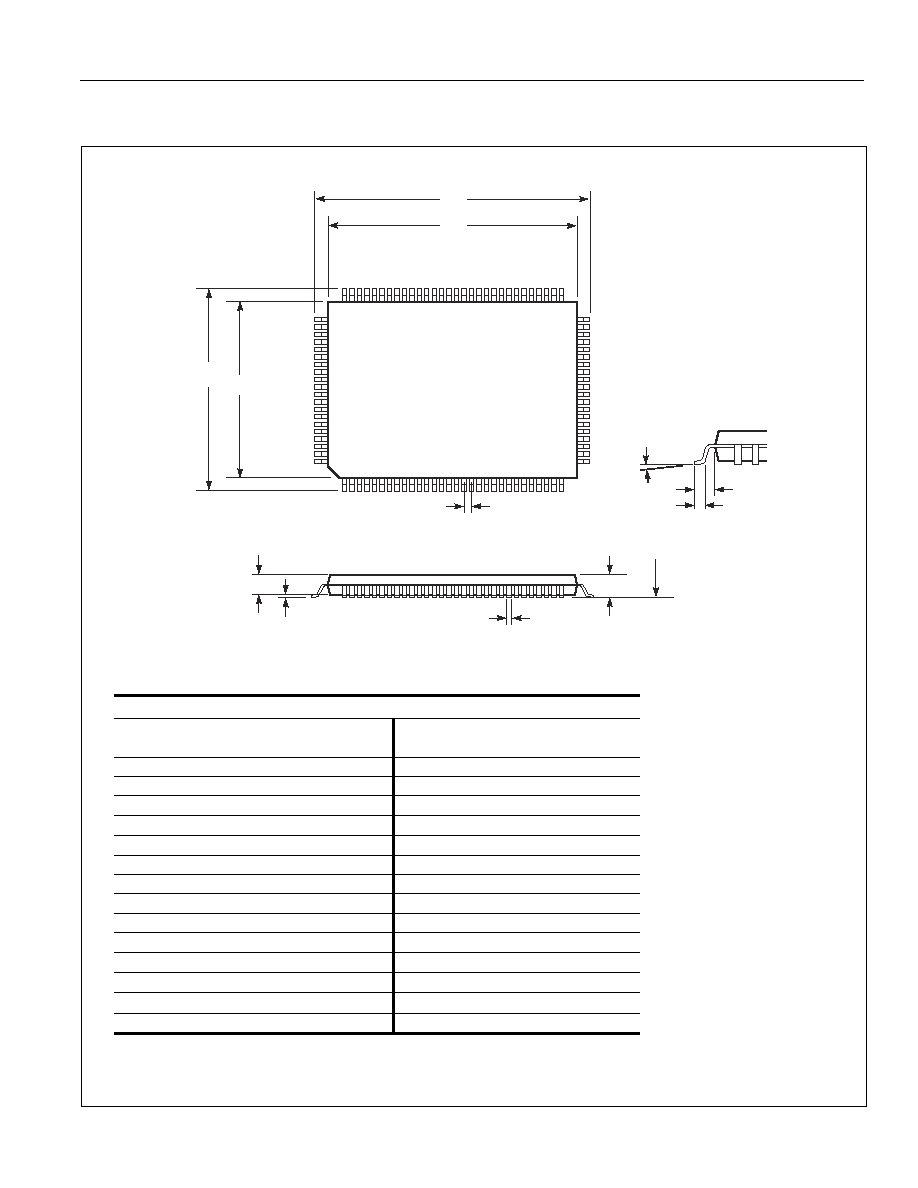
Integrated Silicon Solution, Inc. -- 1-800-379-4774
PACKAGING INFORMATION
ISSI
Æ
PK13197LQ Rev. D 05/08/03
TQFP (Thin Quad Flat Pack Package)
Package Code: TQ
Thin Quad Flat Pack (TQ)
Millimeters
Inches
Millimeters
Inches
Symbol
Min
Max
Min
Max
Min
Max
Min
Max
Ref. Std.
No. Leads (N)
100
128
A
--
1.60
--
0.063
--
1.60
--
0.063
A1
0.05
0.15
0.002
0.006
0.05
0.15
0.002
0.006
A2
1.35
1.45
0.053
0.057
1.35
1.45
0.053
0.057
b
0.22
0.38
0.009
0.015
0.17
0.27
0.007
0.011
D
21.90
22.10
0.862
0.870
21.80
22.20
0.858
0.874
D1
19.90
20.10
0.783
0.791
19.90
20.10
0.783
0.791
E
15.90
16.10
0.626
0.634
15.80
16.20
0.622
0.638
E1
13.90
14.10
0.547
0.555
13.90
14.10
0.547
0.555
e
0.65 BSC
0.026 BSC
0.50 BSC
0.020 BSC
L
0.45
0.75
0.018
0.030
0.45
0.75
0.018
0.030
L1
1.00 REF.
0.039 REF.
1.00 REF.
0.039 REF.
C
0
o
7
o
0
o
7
o
0
o
7
o
0
o
7
o
Notes:
1. All dimensioning and
tolerancing conforms to
ANSI Y14.5M-1982.
2. Dimensions D1 and E1 do
not include mold protrusions.
Allowable protrusion is 0.25
mm per side. D1 and E1 do
include mold mismatch and
are determined at datum
plane -H-.
3. Controlling dimension:
millimeters.
D
D1
E
E1
1
N
A2
A
A1
e
b
SEATING
PLANE
C
L1
L