
Integrated Silicon Solution, Inc. -- www.issi.com --
1-800-379-4774
1
Rev. 00C
09/12/05
ISSI
Æ
Copyright © 2005 Integrated Silicon Solution, Inc. All rights reserved. ISSI reserves the right to make changes to this specification and its products at any time without notice. ISSI assumes no liability
arising out of the application or use of any information, products or services described herein. Customers are advised to obtain the latest version of this device specification before relying on any
published information and before placing orders for products.
IS61NLP12832A
IS61NLP12836A/IS61NVP12836A
IS61NLP25618A/IS61NVP25618A
FEATURES
∑ 100 percent bus utilization
∑ No wait cycles between Read and Write
∑ Internal self-timed write cycle
∑ Individual Byte Write Control
∑ Single R/W (Read/Write) control pin
∑ Clock controlled, registered address,
data and control
∑ Interleaved or linear burst sequence control using
MODE input
∑ Three chip enables for simple depth expansion
and address pipelining
∑ Power Down mode
∑ Common data inputs and data outputs
∑
CKE
pin to enable clock and suspend operation
∑ JEDEC 100-pin TQFP, 165-ball PBGA and 119-
ball PBGA packages
∑ Power supply:
NVP: V
DD
2.5V (± 5%), V
DDQ
2.5V (± 5%)
NLP: V
DD
3.3V (± 5%), V
DDQ
3.3V/2.5V (± 5%)
∑ Industrial temperature available
∑ Lead-free available
DESCRIPTION
The 4 Meg 'NLP/NVP' product family feature high-speed,
low-power synchronous static RAMs designed to provide
a burstable, high-performance, 'no wait' state, device for
networking and communications applications. They are
organized as 128K words by 32 bits, 128K words by 36 bits,
and 256K words by 18 bits, fabricated with
ISSI
's advanced
CMOS technology.
Incorporating a 'no wait' state feature, wait cycles are
eliminated when the bus switches from read to write, or
write to read. This device integrates a 2-bit burst counter,
high-speed SRAM core, and high-drive capability outputs
into a single monolithic circuit.
All synchronous inputs pass through registers are controlled
by a positive-edge-triggered single clock input. Operations
may be suspended and all synchronous inputs ignored
when Clock Enable,
CKE
is HIGH. In this state the internal
device will hold their previous values.
All Read, Write and Deselect cycles are initiated by the
ADV input. When the ADV is HIGH the internal burst
counter is incremented. New external addresses can be
loaded when ADV is LOW.
Write cycles are internally self-timed and are initiated by
the rising edge of the clock inputs and when
WE
is LOW.
Separate byte enables allow individual bytes to be written.
A burst mode pin (MODE) defines the order of the burst
sequence. When tied HIGH, the interleaved burst sequence
is selected. When tied LOW, the linear burst sequence is
selected.
128K x 32, 128K x 36, and 256K x 18
4Mb, PIPELINE 'NO WAIT' STATE BUS SRAM
PRELIMINARY INFORMATION
SEPTEMBER 2005
FAST ACCESS TIME
Symbol
Parameter
-250
-200
Units
t
KQ
Clock Access Time
2.6
3.1
ns
t
KC
Cycle Time
4
5
ns
Frequency
250
200
MHz
2
Integrated Silicon Solution, Inc. -- www.issi.com --
1-800-379-4774
Rev. 00C
09/12/05
ISSI
Æ
IS61NLP12832A
IS61NLP12836A/IS61NVP12836A
IS61NLP25618A/IS61NVP25618A
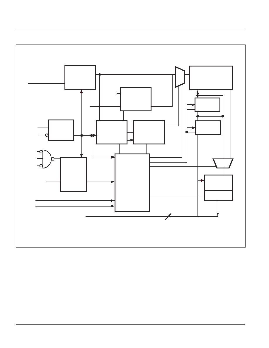
BLOCK DIAGRAM
ADV
WE
}
BWY
X
(X=a,b,c,d or a,b)
CE
CE2
CE2
CONTROL
LOGIC
128Kx32;
128Kx36;
256Kx18
MEMORY ARRAY
WRITE
ADDRESS
REGISTER
WRITE
ADDRESS
REGISTER
CONTROL
LOGIC
OUTPUT
REGISTER
BUFFER
ADDRESS
REGISTER
x 32/x 36: A [0:16] or
x 18: A [0:17]
CLK
CKE
A2-A16 or A2-A17
A0-A1
A'0-A'1
BURST
ADDRESS
COUNTER
MODE
DATA-IN
REGISTER
DATA-IN
REGISTER
CONTROL
REGISTER
OE
ZZ
32, 36 or 18
K
K
DQx/DQPx
K
K
Integrated Silicon Solution, Inc. -- www.issi.com --
1-800-379-4774
3
Rev. 00C
09/12/05
ISSI
Æ
IS61NLP12832A
IS61NLP12836A/IS61NVP12836A
IS61NLP25618A/IS61NVP25618A
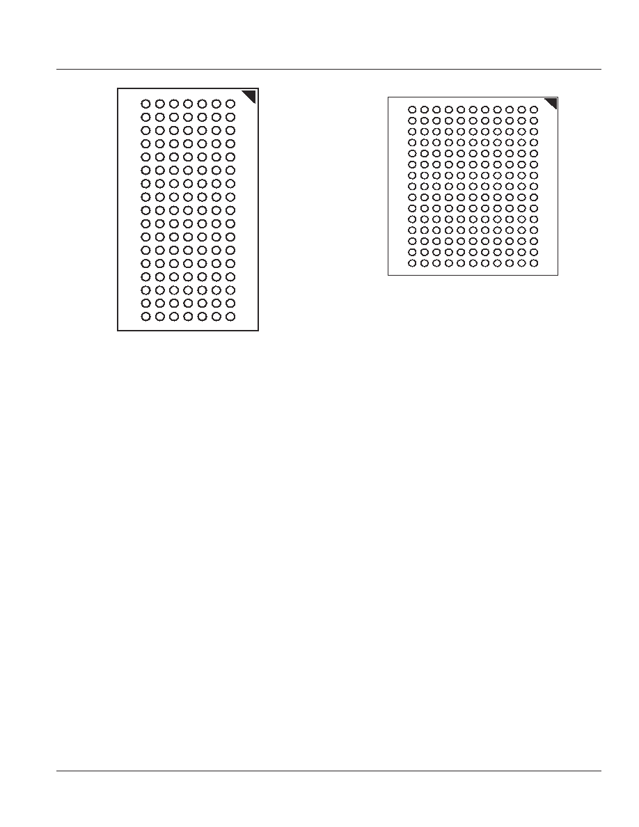
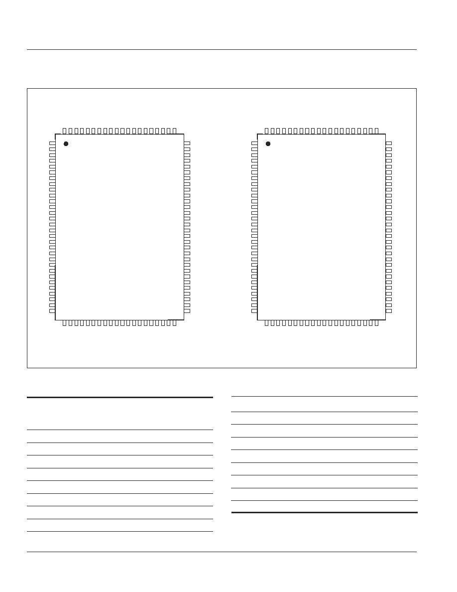
Bottom View
165-Ball, 13 mm x 15mm BGA
1 mm Ball Pitch, 11 x 15 Ball Array
Bottom View
119-Ball, 14 mm x 22 mm BGA
1 mm Ball Pitch, 7 x 17 Ball Array
4
Integrated Silicon Solution, Inc. -- www.issi.com --
1-800-379-4774
Rev. 00C
09/12/05
ISSI
Æ
IS61NLP12832A
IS61NLP12836A/IS61NVP12836A
IS61NLP25618A/IS61NVP25618A
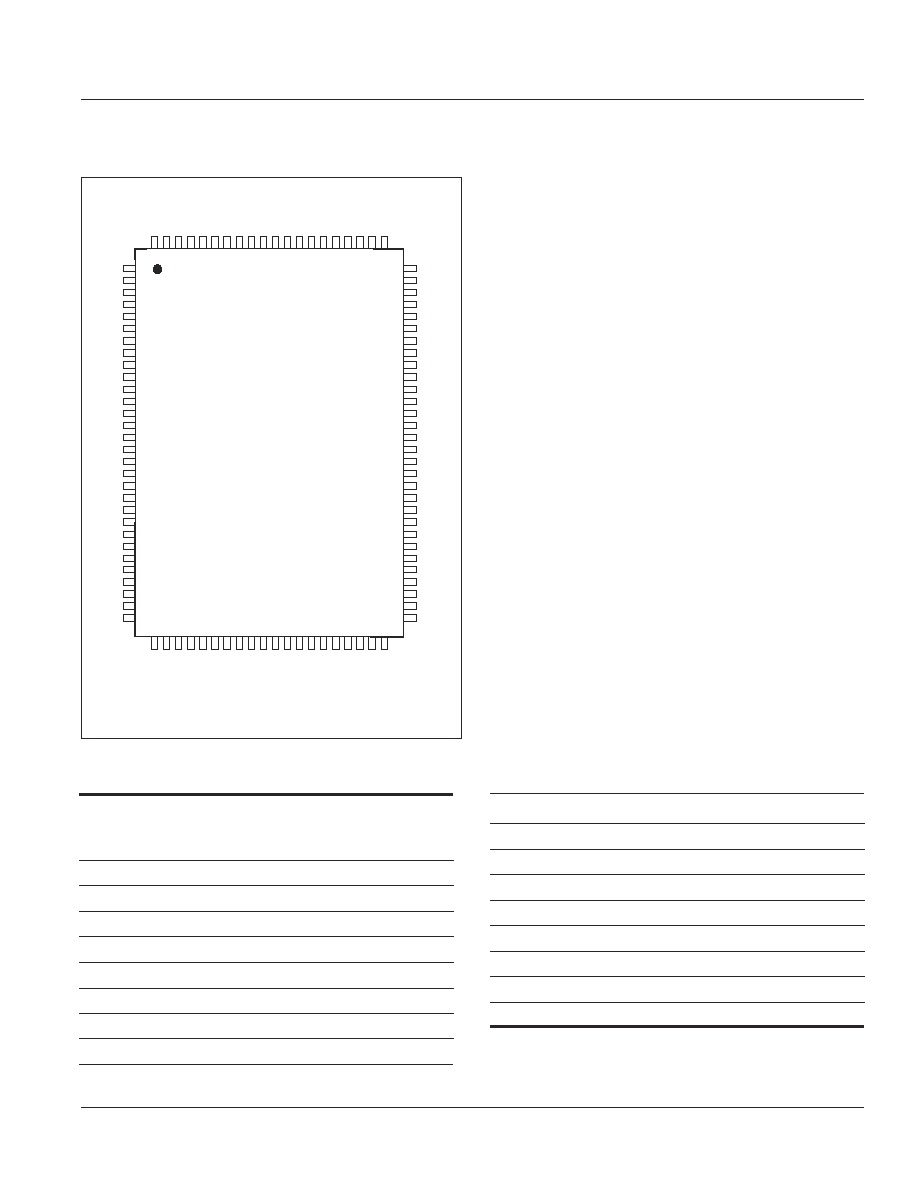
PIN CONFIGURATION -- 128K
X
36, 165-Ball PBGA (TOP VIEW)
1
2
3
4
5
6
7
8
9
10
11
A
NC
A
CE
BW
c
BW
b
CE
2
CKE
ADV
NC
A
NC
B
NC
A
CE2
BW
d
BW
a
CLK
WE
OE
NC
A
NC
C
DQPc
NC
V
DDQ
V
SS
V
SS
V
SS
V
SS
V
SS
V
DDQ
NC
DQPb
D
DQc
DQc
V
DDQ
V
DD
V
SS
V
SS
V
SS
V
DD
V
DDQ
DQb
DQb
E
DQc
DQc
V
DDQ
V
DD
V
SS
V
SS
V
SS
V
DD
V
DDQ
DQb
DQb
F
DQc
DQc
V
DDQ
V
DD
V
SS
V
SS
V
SS
V
DD
V
DDQ
DQb
DQb
G
DQc
DQc
V
DDQ
V
DD
V
SS
V
SS
V
SS
V
DD
V
DDQ
DQb
DQb
H
NC
NC
NC
V
DD
V
SS
V
SS
V
SS
V
DD
NC
NC
ZZ
J
DQd
DQd
V
DDQ
V
DD
V
SS
V
SS
V
SS
V
DD
V
DDQ
DQa
DQa
K
DQd
DQd
V
DDQ
V
DD
V
SS
V
SS
V
SS
V
DD
V
DDQ
DQa
DQa
L
DQd
DQd
V
DDQ
V
DD
V
SS
V
SS
V
SS
V
DD
V
DDQ
DQa
DQa
M
DQd
DQd
V
DDQ
V
DD
V
SS
V
SS
V
SS
V
DD
V
DDQ
DQa
DQa
N
DQPd
NC
V
DDQ
V
SS
NC
NC
NC
V
SS
V
DDQ
NC
DQPa
P
NC
NC
A
A
NC
A1*
NC
A
A
A
NC
R
MODE
NC
A
A
NC
A0*
NC
A
A
A
A
Note:
A0 and A1 are the two least significant bits (LSB) of the address field and set the internal burst counter if burst is desired.
PIN DESCRIPTIONS
Symbol
Pin Name
A
Address Inputs
A0, A1
Synchronous Burst Address Inputs
ADV
Synchronous Burst Address Advance/
Load
WE
Synchronous Read/Write Control
Input
CLK
Synchronous Clock
CKE
Clock Enable
CE
,
CE2
, CE2 Synchronous Chip Enable
BW
x (x=a-d)
Synchronous Byte Write Inputs
OE
Output Enable
ZZ
Power Sleep Mode
MODE
Burst Sequence Selection
V
DD
3.3V/2.5V Power Supply
NC
No Connect
DQx
Data Inputs/Outputs
DQPx
Parity Data I/O
V
DDQ
Isolated output Power Supply
3.3V/2.5V
V
SS
Ground
Integrated Silicon Solution, Inc. -- www.issi.com --
1-800-379-4774
5
Rev. 00C
09/12/05
ISSI
Æ
IS61NLP12832A
IS61NLP12836A/IS61NVP12836A
IS61NLP25618A/IS61NVP25618A
119-PIN PBGA PACKAGE CONFIGURATION 128K x 36 (TOP VIEW)
1
2
3
4
5
6
7
A
A
BW
b
B
NC
C
NC
D
DQc
DQPc
Vss
E
DQc
DQc
Vss
F
V
DDQ
DQc
G
DQc
DQc
H
DQc
DQc
J
V
DDQ
V
DD
K
DQd
DQd
L
DQd
DQd
M
V
DDQ
DQd
N
DQd
DQd
Vss
P
NC
DQPd
R
A
CE2
MODE
A
0
*
A
A
A
V
SS
V
SS
V
SS
V
SS
BW
d
V
SS
V
SS
V
SS
NC
NC
V
DD
V
DD
V
DD
V
DD
NC
Vss
Vss
Vss
Vss
Vss
NC
CE
2
NC
A
NC
T
U
V
DDQ
NC
V
DDQ
DQd
A
NC
NC
NC
A
A
BW
c
NC
A
1
*
CKE
NC
CLK
NC
WE
NC
OE
CE
NC
ADV
NC
A
NC
BW
a
A
A
A
DQPa
DQa
DQa
DQa
DQa
DQb
DQb
DQb
DQb
DQPb
A
A
V
DDQ
ZZ
DQa
DQa
V
DDQ
DQa
DQa
V
DDQ
DQb
DQb
V
DDQ
DQb
DQb
NC
V
DDQ
V
SS
Note:
A0 and A1 are the two least significant bits(LSB) of the address field and set the internal burst counter if burst is desired.
PIN DESCRIPTIONS
Symbol
Pin Name
A
Address Inputs
A0, A1
Synchronous Burst Address Inputs
ADV
Synchronous Burst Address Advance/
Load
WE
Synchronous Read/Write Control Input
CLK
Synchronous Clock
CKE
Clock Enable
CE
Synchronous Chip Select
CE
2
Synchronous Chip Select
CE2
Synchronous Chip Select
BW
x (x=a-d)
Synchronous Byte Write Inputs
OE
Output Enable
ZZ
Power Sleep Mode
MODE
Burst Sequence Selection
V
DD
Power Supply
V
SS
Ground
NC
No Connect
DQa-DQd
Data Inputs/Outputs
DQPa-Pd
Parity Data I/O
V
DDQ
Output Power Supply

6
Integrated Silicon Solution, Inc. -- www.issi.com --
1-800-379-4774
Rev. 00C
09/12/05
ISSI
Æ
IS61NLP12832A
IS61NLP12836A/IS61NVP12836A
IS61NLP25618A/IS61NVP25618A
165-PIN PBGA PACKAGE CONFIGURATION 256K x 18 (TOP VIEW)
PIN DESCRIPTIONS
Symbol
Pin Name
A
Address Inputs
A0, A1
Synchronous Burst Address Inputs
ADV
Synchronous Burst Address Advance/
Load
WE
Synchronous Read/Write Control
Input
CLK
Synchronous Clock
CKE
Clock Enable
CE
,
CE2
, CE2 Synchronous Chip Enable
BW
x (x=a,b)
Synchronous Byte Write Inputs
OE
Output Enable
ZZ
Power Sleep Mode
1
2
3
4
5
6
7
8
9
10
11
A
A
BW
b
CKE
B
NC
A
WE
OE
C
NC
NC
Vss
Vss
D
NC
DQb
Vss
Vss
NC
E
NC
DQb
Vss
Vss
Vss
F
NC
DQb
NC
G
NC
DQb
NC
NC
H
NC
NC
V
DDQ
J
DQb
NC
DQa
K
DQb
NC
L
DQb
NC
Vss
M
DQb
NC
Vss
N
DQPb
NC
Vss
Vss
NC
P
NC
NC
A
1
*
NC
R
MODE
A
NC
CE2
Vss
Vss
Vss
Vss
Vss
Vss
Vss
Vss
NC
NC
A
A
A
A
A
A
A
A
A
A
A
NC
NC
A
A
CE
V
DDQ
V
DDQ
V
DDQ
V
DDQ
V
DDQ
V
DDQ
V
DDQ
V
DDQ
V
DDQ
V
DDQ
NC
NC
V
DD
V
DD
V
DD
V
DD
V
DD
V
DD
V
DD
V
DD
V
DD
NC
BW
a
Vss
Vss
Vss
Vss
Vss
Vss
Vss
Vss
NC
NC
NC
CE
2
CLK
Vss
NC
A
0
*
NC
Vss
Vss
Vss
Vss
Vss
Vss
ADV
V
DD
V
DD
V
DD
V
DD
V
DD
V
DD
V
DD
V
DD
V
DD
V
DDQ
V
DDQ
V
DDQ
V
DDQ
V
DDQ
V
DDQ
V
DDQ
V
DDQ
V
DDQ
NC
NC
NC
DQa
DQa
DQa
NC
NC
NC
NC
NC
NC
NC
ZZ
DQa
DQa
DQa
DQa
DQPa
Note:
A0 and A1 are the two least significant bits (LSB) of the address field and set the internal burst counter if burst is desired.
MODE
Burst Sequence Selection
V
DD
3.3V/2.5V Power Supply
NC
No Connect
DQx
Data Inputs/Outputs
DQPx
Parity Data I/O
V
DDQ
Isolated output Power Supply
3.3V/2.5V
V
SS
Ground
Integrated Silicon Solution, Inc. -- www.issi.com --
1-800-379-4774
7
Rev. 00C
09/12/05
ISSI
Æ
IS61NLP12832A
IS61NLP12836A/IS61NVP12836A
IS61NLP25618A/IS61NVP25618A
119-PIN PBGA PACKAGE CONFIGURATION 256K x 18 (TOP VIEW)
PIN DESCRIPTIONS
Symbol
Pin Name
A
Address Inputs
A0, A1
Synchronous Burst Address Inputs
ADV
Synchronous Burst Address Advance/
Load
WE
Synchronous Read/Write Control Input
CLK
Synchronous Clock
CKE
Clock Enable
CE
Synchronous Chip Select
CE
2
Synchronous Chip Select
CE2
Synchronous Chip Select
BW
x (x=a,b)
Synchronous Byte Write Inputs
OE
Output Enable
ZZ
Power Sleep Mode
MODE
Burst Sequence Selection
V
DD
Power Supply
V
SS
Ground
NC
No Connect
DQa-DQb
Data Inputs/Outputs
DQPa-Pb
Parity Data I/O
V
DDQ
Output Power Supply
1
2
3
4
5
6
7
A
A
B
NC
C
NC
D
DQb
Vss
E
DQb
Vss
F
V
DDQ
G
DQb
H
DQb
J
V
DDQ
V
DD
K
DQb
L
DQb
M
V
DDQ
DQb
N
DQb
NC
Vss
P
NC
DQPb
R
A
CE2
MODE
A
A
0
*
A
A
V
SS
V
SS
V
SS
V
SS
NC
V
SS
V
SS
NC
NC
V
DD
V
DD
V
DD
V
DD
NC
Vss
Vss
Vss
Vss
Vss
NC
CE
2
NC
A
NC
T
U
V
DDQ
NC
V
DDQ
A
NC
NC
NC
A
A
BW
b
NC
A
1
*
CKE
NC
CLK
NC
WE
NC
OE
CE
NC
ADV
NC
A
NC
BW
a
A
A
A
DQPa
DQa
DQa
DQa
DQa
A
A
V
DDQ
ZZ
DQa
DQa
V
DDQ
DQa
DQa
V
DDQ
V
DDQ
NC
V
DDQ
NC
NC
NC
NC
NC
NC
NC
NC
A
V
SS
V
SS
NC
NC
NC
NC
NC
NC
NC
NC
NC
Note:
A0 and A1 are the two least significant bits(LSB) of the address field and set the internal burst counter if burst is desired.
8
Integrated Silicon Solution, Inc. -- www.issi.com --
1-800-379-4774
Rev. 00C
09/12/05
ISSI
Æ
IS61NLP12832A
IS61NLP12836A/IS61NVP12836A
IS61NLP25618A/IS61NVP25618A
PIN CONFIGURATION
100-Pin TQFP
128K x 32
1
2
3
4
5
6
7
8
9
10
11
12
13
14
15
16
17
18
19
20
21
22
23
24
25
26
27
28
29
30
80
79
78
77
76
75
74
73
72
71
70
69
68
67
66
65
64
63
62
61
60
59
58
57
56
55
54
53
52
51
100 99 98 97 96 95 94 93 92 91 90 89 88 87 86 85 84 83 82 81
31 32 33 34 35 36 37 38 39 40 41 42 43 44 45 46 47 48 49 50
DQPb
DQb
DQb
V
DDQ
Vss
DQb
DQb
DQb
DQb
Vss
V
DDQ
DQb
DQb
Vss
NC
V
DD
ZZ
DQa
DQa
V
DDQ
Vss
DQa
DQa
DQa
DQa
Vss
V
DDQ
DQa
DQa
DQPa
DQPc
DQc
DQc
V
DDQ
Vss
DQc
DQc
DQc
DQc
Vss
V
DDQ
DQc
DQc
NC
V
DD
NC
Vss
DQd
DQd
V
DDQ
Vss
DQd
DQd
DQd
DQd
Vss
V
DDQ
DQd
DQd
DQPd
A
A
CE
CE2
BWd
BWc
BWb
BWa
CE2
V
DD
Vss
CLK
WE
CKE
OE
AD
V
NC
NC
A
A
MODE
A
A
A
A
A1
A0
NC
NC
Vss
V
DD
NC
NC
A
A
A
A
A
A
A
128K x 36
PIN DESCRIPTIONS
A0, A1
Synchronous Address Inputs. These
pins must tied to the two LSBs of the
address bus.
A
Synchronous Address Inputs
CLK
Synchronous Clock
ADV
Synchronous Burst Address Advance
BW
a-
BW
d
Synchronous Byte Write Enable
WE
Write Enable
CKE
Clock Enable
Vss
Ground for Core
NC
Not Connected
CE
, CE2,
CE2
Synchronous Chip Enable
OE
Output Enable
DQa-DQd
Synchronous Data Input/Output
DQPa-DQPd
Parity Data I/O
MODE
Burst Sequence Selection
V
DD
+3.3V/2.5V Power Supply
V
SS
Ground for output Buffer
V
DDQ
Isolated Output Buffer Supply: +3.3V/2.5V
ZZ
Snooze Enable
1
2
3
4
5
6
7
8
9
10
11
12
13
14
15
16
17
18
19
20
21
22
23
24
25
26
27
28
29
30
80
79
78
77
76
75
74
73
72
71
70
69
68
67
66
65
64
63
62
61
60
59
58
57
56
55
54
53
52
51
100 99 98 97 96 95 94 93 92 91 90 89 88 87 86 85 84 83 82 81
31 32 33 34 35 36 37 38 39 40 41 42 43 44 45 46 47 48 49 50
NC
DQb
DQb
V
DDQ
Vss
DQb
DQb
DQb
DQb
Vss
V
DDQ
DQb
DQb
Vss
NC
V
DD
ZZ
DQa
DQa
V
DDQ
Vss
DQa
DQa
DQa
DQa
Vss
V
DDQ
DQa
DQa
NC
NC
DQc
DQc
V
DDQ
Vss
DQc
DQc
DQc
DQc
Vss
V
DDQ
DQc
DQc
NC
V
DD
NC
Vss
DQd
DQd
V
DDQ
Vss
DQd
DQd
DQd
DQd
Vss
V
DDQ
DQd
DQd
NC
A
A
CE
CE2
BWd
BWc
BWb
BWa
CE2
V
DD
Vss
CLK
WE
CKE
OE
AD
V
NC
NC
A
A
MODE
A
A
A
A
A1
A0
NC
NC
Vss
V
DD
NC
NC
A
A
A
A
A
A
A
Integrated Silicon Solution, Inc. -- www.issi.com --
1-800-379-4774
9
Rev. 00C
09/12/05
ISSI
Æ
IS61NLP12832A
IS61NLP12836A/IS61NVP12836A
IS61NLP25618A/IS61NVP25618A
PIN CONFIGURATION
100-Pin TQFP
256K x 18
1
2
3
4
5
6
7
8
9
10
11
12
13
14
15
16
17
18
19
20
21
22
23
24
25
26
27
28
29
30
80
79
78
77
76
75
74
73
72
71
70
69
68
67
66
65
64
63
62
61
60
59
58
57
56
55
54
53
52
51
100 99 98 97 96 95 94 93 92 91 90 89 88 87 86 85 84 83 82 81
31 32 33 34 35 36 37 38 39 40 41 42 43 44 45 46 47 48 49 50
A
NC
NC
V
DDQ
Vss
NC
DQPa
DQa
DQa
Vss
V
DDQ
DQa
DQa
Vss
NC
V
DD
ZZ
DQa
DQa
V
DDQ
Vss
DQa
DQa
NC
NC
Vss
V
DDQ
NC
NC
NC
NC
NC
NC
V
DDQ
Vss
NC
NC
DQb
DQb
Vss
V
DDQ
DQb
DQb
NC
V
DD
NC
Vss
DQb
DQb
V
DDQ
Vss
DQb
DQb
DQPb
NC
Vss
V
DDQ
NC
NC
NC
A
A
CE
CE2
NC
NC
BW
b
BW
a
CE2
V
DD
Vss
CLK
WE
CKE
OE
ADV
NC
NC
A
A
MODE
A
A
A
A
A1
A0
NC
NC
Vss
V
DD
NC
NC
A
A
A
A
A
A
A
PIN DESCRIPTIONS
A0, A1
Synchronous Address Inputs. These
pins must tied to the two LSBs of the
address bus.
A
Synchronous Address Inputs
CLK
Synchronous Clock
ADV
Synchronous Burst Address Advance
BW
a-
BW
d
Synchronous Byte Write Enable
WE
Write Enable
CKE
Clock Enable
Vss
Ground for Core
NC
Not Connected
CE
, CE2,
CE2
Synchronous Chip Enable
OE
Output Enable
DQa-DQd
Synchronous Data Input/Output
DQPa-DQPd
Parity Data I/O
MODE
Burst Sequence Selection
V
DD
+3.3V/2.5V Power Supply
V
SS
Ground for output Buffer
V
DDQ
Isolated Output Buffer Supply: +3.3V/2.5V
ZZ
Snooze Enable

10
Integrated Silicon Solution, Inc. -- www.issi.com --
1-800-379-4774
Rev. 00C
09/12/05
ISSI
Æ
IS61NLP12832A
IS61NLP12836A/IS61NVP12836A
IS61NLP25618A/IS61NVP25618A
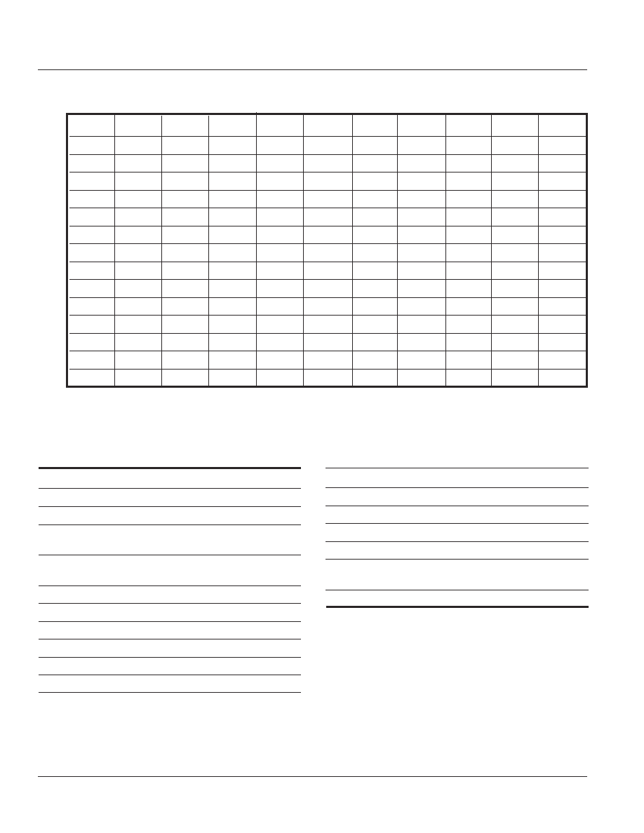
SYNCHRONOUS TRUTH TABLE
(1)
Address
Operation
Used
CE
CE
CE
CE
CE
CE2
CE
CE
CE
CE
CE
2
ADV
WE
WE
WE
WE
WE
BW
BW
BW
BW
BW
x
OE
OE
OE
OE
OE
CKE
CKE
CKE
CKE
CKE
CLK
Not Selected
N/A
H
X
X
L
X
X
X
L
Not Selected
N/A
X
L
X
L
X
X
X
L
Not Selected
N/A
X
X
H
L
X
X
X
L
Not Selected Continue
N/A
X
X
X
H
X
X
X
L
Begin Burst Read
External Address
L
H
L
L
H
X
L
L
Continue Burst Read
Next Address
X
X
X
H
X
X
L
L
NOP/Dummy Read
External Address
L
H
L
L
H
X
H
L
Dummy Read
Next Address
X
X
X
H
X
X
H
L
Begin Burst Write
External Address
L
H
L
L
L
L
X
L
Continue Burst Write
Next Address
X
X
X
H
X
L
X
L
NOP/Write Abort
N/A
L
H
L
L
L
H
X
L
Write Abort
Next Address
X
X
X
H
X
H
X
L
Ignore Clock
Current Address
X
X
X
X
X
X
X
H
Notes:
1. "X" means don't care.
2. The rising edge of clock is symbolized by
3. A continue deselect cycle can only be entered if a deselect cycle is executed first.
4.
WE
= L means Write operation in Write Truth Table.
WE
= H means Read operation in Write Truth Table.
5. Operation finally depends on status of asynchronous pins (ZZ and
OE
).
BURST
READ
DESELECT
BURST
WRITE
BEGIN
READ
BEGIN
WRITE
READ
WRITE
READ
WRITE
BURST
BURST
BURST
DS
DS
DS
READ
DS
DS
READ
WRITE
WRITE
BURST
BURST
WRITE
READ
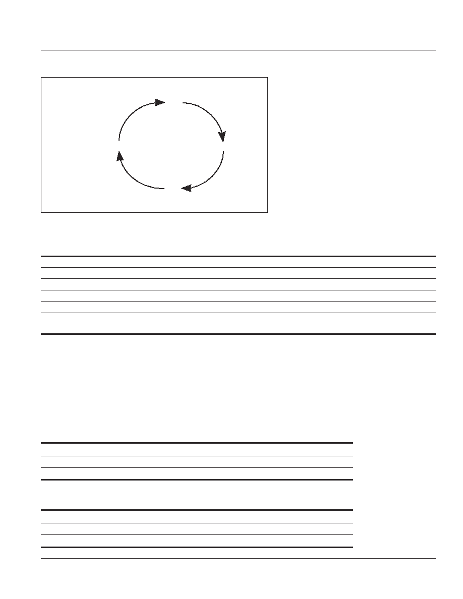
STATE DIAGRAM

Integrated Silicon Solution, Inc. -- www.issi.com --
1-800-379-4774
11
Rev. 00C
09/12/05
ISSI
Æ
IS61NLP12832A
IS61NLP12836A/IS61NVP12836A
IS61NLP25618A/IS61NVP25618A
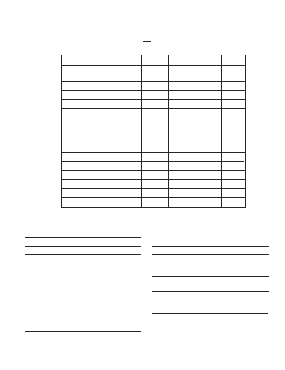
ASYNCHRONOUS TRUTH TABLE
(1)
Operation
ZZ
OE
OE
OE
OE
OE
I/O STATUS
Sleep Mode
H
X
High-Z
Read
L
L
DQ
L
H
High-Z
Write
L
X
Din, High-Z
Deselected
L
X
High-Z
Notes:
1. X means "Don't Care".
2. For write cycles following read cycles, the output buffers must be disabled with
OE
, otherwise data bus
contention will occur.
3. Sleep Mode means power Sleep Mode where stand-by current does not depend on cycle time.
4. Deselected means power Sleep Mode where stand-by current depends on cycle time.
WRITE TRUTH TABLE
(x18)
Operation
WE
WE
WE
WE
WE
BW
BW
BW
BW
BW
a
BW
BW
BW
BW
BW
b
READ
H
X
X
WRITE BYTE a
L
L
H
WRITE BYTE b
L
H
L
WRITE ALL BYTEs
L
L
L
WRITE ABORT/NOP
L
H
H
Notes:
1. X means "Don't Care".
2. All inputs in this table must beet setup and hold time around the rising edge of CLK.

12
Integrated Silicon Solution, Inc. -- www.issi.com --
1-800-379-4774
Rev. 00C
09/12/05
ISSI
Æ
IS61NLP12832A
IS61NLP12836A/IS61NVP12836A
IS61NLP25618A/IS61NVP25618A
INTERLEAVED BURST ADDRESS TABLE
(MODE = V
DD
or NC)
External Address
1st Burst Address
2nd Burst Address
3rd Burst Address
A1 A0
A1 A0
A1 A0
A1 A0
00
01
10
11
01
00
11
10
10
11
00
01
11
10
01
00
WRITE TRUTH TABLE
(x32/x36)
Operation
WE
WE
WE
WE
WE
BW
BW
BW
BW
BW
a
BW
BW
BW
BW
BW
b
BW
BW
BW
BW
BW
c
BW
BW
BW
BW
BW
d
READ
H
X
X
X
X
WRITE BYTE a
L
L
H
H
H
WRITE BYTE b
L
H
L
H
H
WRITE BYTE c
L
H
H
L
H
WRITE BYTE d
L
H
H
H
L
WRITE ALL BYTEs
L
L
L
L
L
WRITE ABORT/NOP
L
H
H
H
H
Notes
:
1. X means "Don't Care".
2. All inputs in this table must beet setup and hold time around the rising edge of CLK.
Integrated Silicon Solution, Inc. -- www.issi.com --
1-800-379-4774
13
Rev. 00C
09/12/05
ISSI
Æ
IS61NLP12832A
IS61NLP12836A/IS61NVP12836A
IS61NLP25618A/IS61NVP25618A
LINEAR BURST ADDRESS TABLE
(MODE = V
SS
)
ABSOLUTE MAXIMUM RATINGS
(1)
Symbol
Parameter
Value
Unit
T
STG
Storage Temperature
≠65 to +150
∞C
P
D
Power Dissipation
1.6
W
I
OUT
Output Current (per I/O)
100
mA
V
IN
, V
OUT
Voltage Relative to V
SS
for I/O Pins
≠0.5 to V
DDQ
+ 0.5
V
V
IN
Voltage Relative to V
SS
for
≠0.5 to 4.6
V
for Address and Control Inputs
Notes:
1. Stress greater than those listed under ABSOLUTE MAXIMUM RATINGS may cause permanent damage to the device. This is
a stress rating only and functional operation of the device at these or any other conditions above those indicated in the
operational sections of this specification is not implied. Exposure to absolute maximum rating conditions for extended periods
may affect reliability.
2. This device contains circuity to protect the inputs against damage due to high static voltages or electric fields; however,
precautions may be taken to avoid application of any voltage higher than maximum rated voltages to this high-impedance
circuit.
3. This device contains circuitry that will ensure the output devices are in High-Z at power up.
0,0
1,0
0,1
A1', A0' = 1,1
OPERATING RANGE (IS61NLPx)
Range
Ambient Temperature
V
DD
V
DDQ
Commercial
0∞C to +70∞C
3.3V ± 5%
3.3V / 2.5V ± 5%
Industrial
-40∞C to +85∞C
3.3V ± 5%
3.3V / 2.5V ± 5%
OPERATING RANGE (IS61NVPx)
Range
Ambient Temperature
V
DD
V
DDQ
Commercial
0∞C to +70∞C
2.5V ± 5%
2.5V ± 5%
Industrial
-40∞C to +85∞C
2.5V ± 5%
2.5V ± 5%

14
Integrated Silicon Solution, Inc. -- www.issi.com --
1-800-379-4774
Rev. 00C
09/12/05
ISSI
Æ
IS61NLP12832A
IS61NLP12836A/IS61NVP12836A
IS61NLP25618A/IS61NVP25618A
POWER SUPPLY CHARACTERISTICS
(1)
(Over Operating Range)
-250
-200
MAX
MAX
Symbol Parameter
Test Conditions
Temp. range
x18
x32/x36
x18
x32/x36
Unit
I
CC
AC Operating
Device Selected,
Com.
225
225
200
200
mA
Supply Current
OE
= V
IH
, ZZ
V
IL
,
Ind.
250
250
210
210
All Inputs
0.2V or
V
DD
≠ 0.2V,
Cycle Time
t
KC
min.
I
SB
Standby Current
Device Deselected,
Com.
90
90
90
90
mA
TTL Input
V
DD
= Max.,
Ind.
100
100
100
100
All Inputs
V
IL
or
V
IH
,
ZZ
V
IL
, f = Max.
I
SBI
Standby Current
Device Deselected,
Com.
70
70
70
70
mA
CMOS Input
V
DD
= Max.,
Ind.
75
75
75
75
V
IN
V
SS
+ 0.2V or
V
DD
≠ 0.2V
typ.
(2)
40
f = 0
I
SB
2
Sleep Mode
ZZ>V
IH
Com.
30
30
30
30
mA
Ind.
35
35
35
35
typ.
(2)
20
Note:
1. MODE pin has an internal pullup and should be tied to V
DD
or V
SS
. It exhibits ±100µA maximum leakage current when tied to
V
SS
+ 0.2V or
V
DD
≠ 0.2V.
2. Typical values are measured at V
DD
= 3.3V, T
A
= 25
o
C and not 100% tested.
DC ELECTRICAL CHARACTERISTICS
(Over Operating Range)
3.3V
2.5V
Symbol
Parameter
Test Conditions
Min.
Max.
Min.
Max.
Unit
V
OH
Output HIGH Voltage
I
OH
= ≠4.0 mA (3.3V)
2.4
--
2.0
--
V
I
OH
= ≠1.0 mA
(2.5V)
V
OL
Output LOW Voltage
I
OL
= 8.0 mA (3.3V)
--
0.4
--
0.4
V
I
OL
= 1.0 mA (2.5V)
V
IH
(1)
Input HIGH Voltage
2.0
V
DD
+ 0.3
1.7
V
DD
+ 0.3
V
V
IL
(1)
Input LOW Voltage
≠0.3
0.8
≠0.3
0.7
V
I
LI
Input Leakage Current
V
SS
V
IN
V
DD
(1)
≠5
5
≠5
5
µA
I
LO
Output Leakage Current
V
SS
V
OUT
V
DDQ
,
OE
= V
IH
≠5
5
≠5
5
µA
Note:
1. Overshoot: V
IH
(AC) < V
DD
+ 2.0V (Pulse width less than t
KC
/2). Undershoot: V
IL
(AC) > -2V (Pulse width less than t
KC
/2).

Integrated Silicon Solution, Inc. -- www.issi.com --
1-800-379-4774
15
Rev. 00C
09/12/05
ISSI
Æ
IS61NLP12832A
IS61NLP12836A/IS61NVP12836A
IS61NLP25618A/IS61NVP25618A
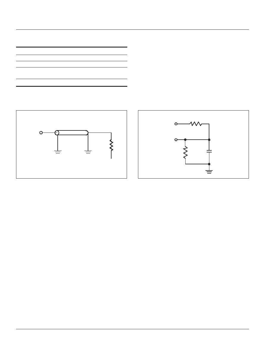
3.3V I/O AC TEST CONDITIONS
Parameter
Unit
Input Pulse Level
0V to 3.0V
Input Rise and Fall Times
1.5 ns
Input and Output Timing
1.5V
and Reference Level
Output Load
See Figures 1 and 2
317
5 pF
Including
jig and
scope
351
OUTPUT
+3.3V
Figure 1
Figure 2
CAPACITANCE
(1,2)
Symbol
Parameter
Conditions
Max.
Unit
C
IN
Input Capacitance
V
IN
= 0V
6
pF
C
OUT
Input/Output Capacitance
V
OUT
= 0V
8
pF
Notes:
1. Tested initially and after any design or process changes that may affect these parameters.
2. Test conditions: T
A
= 25∞C, f = 1 MHz, V
DD
= 3.3V.
3.3V I/O OUTPUT LOAD EQUIVALENT
1.5V
OUTPUT
Zo= 50
50
16
Integrated Silicon Solution, Inc. -- www.issi.com --
1-800-379-4774
Rev. 00C
09/12/05
ISSI
Æ
IS61NLP12832A
IS61NLP12836A/IS61NVP12836A
IS61NLP25618A/IS61NVP25618A
2.5V I/O AC TEST CONDITIONS
Parameter
Unit
Input Pulse Level
0V to 2.5V
Input Rise and Fall Times
1.5 ns
Input and Output Timing
1.25V
and Reference Level
Output Load
See Figures 3 and 4
Z
O
= 50
1.25V
50
OUTPUT
1,667
5 pF
Including
jig and
scope
1,538
OUTPUT
+2.5V
Figure 3
Figure 4
2.5V I/O OUTPUT LOAD EQUIVALENT

Integrated Silicon Solution, Inc. -- www.issi.com --
1-800-379-4774
17
Rev. 00C
09/12/05
ISSI
Æ
IS61NLP12832A
IS61NLP12836A/IS61NVP12836A
IS61NLP25618A/IS61NVP25618A
READ/WRITE CYCLE SWITCHING CHARACTERISTICS
(1)
(Over Operating Range)
-250
-200
Symbol
Parameter
Min.
Max.
Min. Max.
Unit
fmax
Clock Frequency
--
250
--
200
MHz
t
KC
Cycle Time
4.0
--
5
--
ns
t
KH
Clock High Time
1.7
--
2
--
ns
t
KL
Clock Low Time
1.7
--
2
--
ns
t
KQ
Clock Access Time
--
2.6
--
3.1
ns
t
KQX
(2)
Clock High to Output Invalid
0.8
--
1.5
--
ns
t
KQLZ
(2,3)
Clock High to Output Low-Z
0.8
--
1
--
ns
t
KQHZ
(2,3)
Clock High to Output High-Z
--
2.6
--
3.0
ns
t
OEQ
Output Enable to Output Valid
--
2.8
--
3.1
ns
t
OELZ
(2,3)
Output Enable to Output Low-Z
0
--
0
--
ns
t
OEHZ
(2,3)
Output Disable to Output High-Z
--
2.6
--
3.0
ns
t
AS
Address Setup Time
1.2
--
1.4
--
ns
t
WS
Read/Write Setup Time
1.2
--
1.4
--
ns
t
CES
Chip Enable Setup Time
1.2
--
1.4
--
ns
t
SE
Clock Enable Setup Time
1.2
--
1.4
--
ns
t
ADVS
Address Advance Setup Time
1.2
--
1.4
--
ns
t
DS
Data Setup Time
1.2
--
1.4
--
ns
t
AH
Address Hold Time
0.3
--
0.4
--
ns
t
HE
Clock Enable Hold Time
0.3
--
0.4
--
ns
t
WH
Write Hold Time
0.3
--
0.4
--
ns
t
CEH
Chip Enable Hold Time
0.3
--
0.4
--
ns
t
ADVH
Address Advance Hold Time
0.3
--
0.4
--
ns
t
DH
Data Hold Time
0.3
--
0.4
--
ns
t
PDS
ZZ High to Power Down
--
2
--
2
cyc
t
PUS
ZZ Low to Power Down
--
2
--
2
cyc
Notes:
1. Configuration signal MODE is static and must not change during normal operation.
2. Guaranteed but not 100% tested. This parameter is periodically sampled.
3. Tested with load in Figure 2.

18
Integrated Silicon Solution, Inc. -- www.issi.com --
1-800-379-4774
Rev. 00C
09/12/05
ISSI
Æ
IS61NLP12832A
IS61NLP12836A/IS61NVP12836A
IS61NLP25618A/IS61NVP25618A
SLEEP MODE TIMING
SLEEP MODE ELECTRICAL CHARACTERISTICS
Symbol
Parameter
Conditions
Min.
Max.
Unit
I
SB
2
Current during SLEEP MODE
ZZ
V
IH
35
mA
t
PDS
ZZ active to input ignored
2
cycle
t
PUS
ZZ inactive to input sampled
2
cycle
t
ZZI
ZZ active to SLEEP current
2
cycle
t
RZZI
ZZ inactive to exit SLEEP current
0
ns
Don't Care
Deselect or Read Only
Deselect or Read Only
t
RZZI
CLK
ZZ
Isupply
All Inputs
(except ZZ)
Outputs
(Q)
I
SB2
ZZ setup cycle
ZZ recovery cycle
Normal
operation
cycle
t
PDS
t
PUS
t
ZZI
High-Z
Integrated Silicon Solution, Inc. -- www.issi.com --
1-800-379-4774
19
Rev. 00C
09/12/05
ISSI
Æ
IS61NLP12832A
IS61NLP12836A/IS61NVP12836A
IS61NLP25618A/IS61NVP25618A
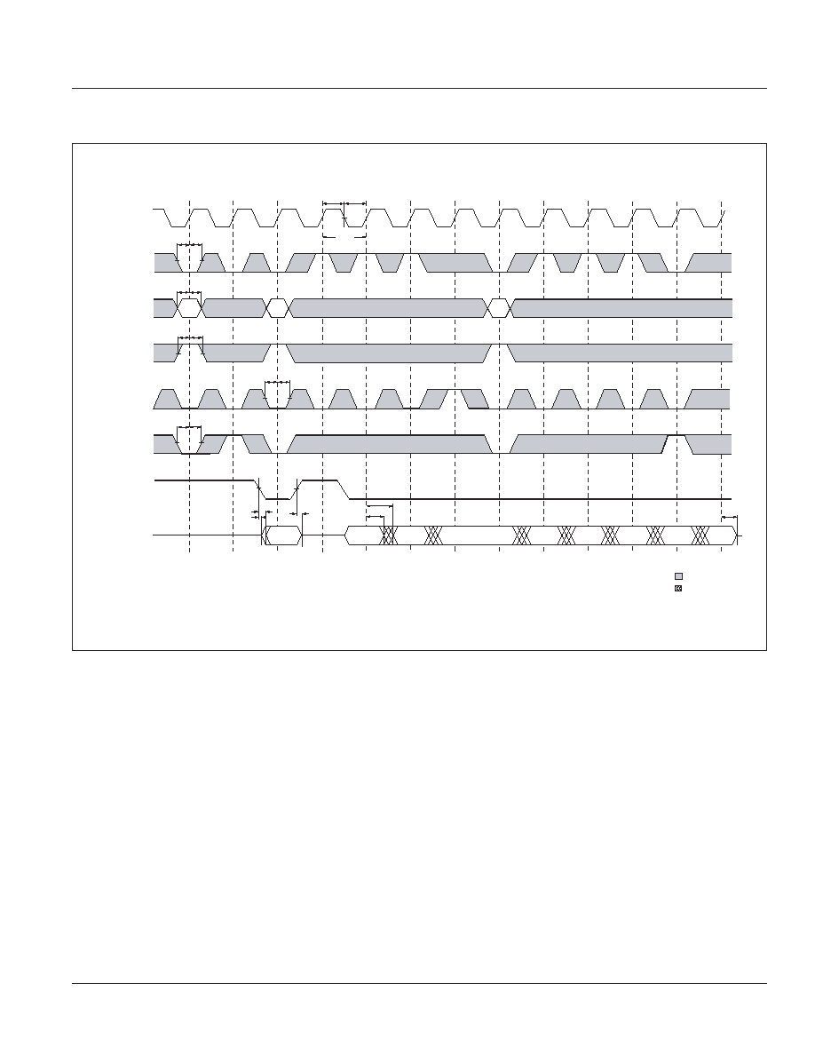
READ CYCLE TIMING
t
KQX
CLK
ADV
Address
WRITE
CKE
CE
OE
Data Out
A1
A2
A3
t
KH
t
KL
t
KC
Q3-3
Q3-4
Q3-2
Q3-1
Q2-4
Q2-3
Q2-2
Q2-1
Don't Care
Undefined
NOTES:
WRITE
= L means
WE
= L and
BW
x = L
WE
= L and
BW
X = L
CE
= L means
CE
1 = L, CE2 = H and
CE
2 = L
CE
= H means
CE
1 = H, or
CE
1 = L and
CE
2 = H, or
CE
1 = L and CE2 = L
t
OEHZ
t
SE
t
HE
t
AS
t
AH
t
WS
t
WH
t
CES
t
CEH
t
ADVS
t
ADVH
t
KQHZ
t
KQ
t
OEQ
t
OEHZ
Q1-1
20
Integrated Silicon Solution, Inc. -- www.issi.com --
1-800-379-4774
Rev. 00C
09/12/05
ISSI
Æ
IS61NLP12832A
IS61NLP12836A/IS61NVP12836A
IS61NLP25618A/IS61NVP25618A
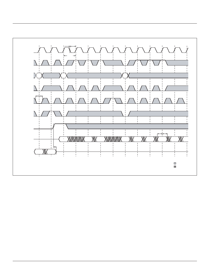
WRITE CYCLE TIMING
t
DS
t
DH
CLK
ADV
Address
WRITE
CKE
CE
OE
Data In
Data Out
A1
A2
A3
t
KH
t
KL
t
KC
t
SE
t
HE
D3-3
D3-4
D3-2
D3-1
D2-4
D2-3
D2-2
D2-1
D1-1
Don't Care
Undefined
NOTES:
WRITE
= L means
WE
= L and
BW
x = L
WE
= L and
BW
X = L
CE
= L means
CE
1 = L, CE2 = H and
CE
2 = L
CE
= H means
CE
1 = H, or
CE
1 = L and
CE
2 = H, or
CE
1 = L and CE2 = L
t
OEHZ
Q0-3 Q0-4

Integrated Silicon Solution, Inc. -- www.issi.com --
1-800-379-4774
21
Rev. 00C
09/12/05
ISSI
Æ
IS61NLP12832A
IS61NLP12836A/IS61NVP12836A
IS61NLP25618A/IS61NVP25618A
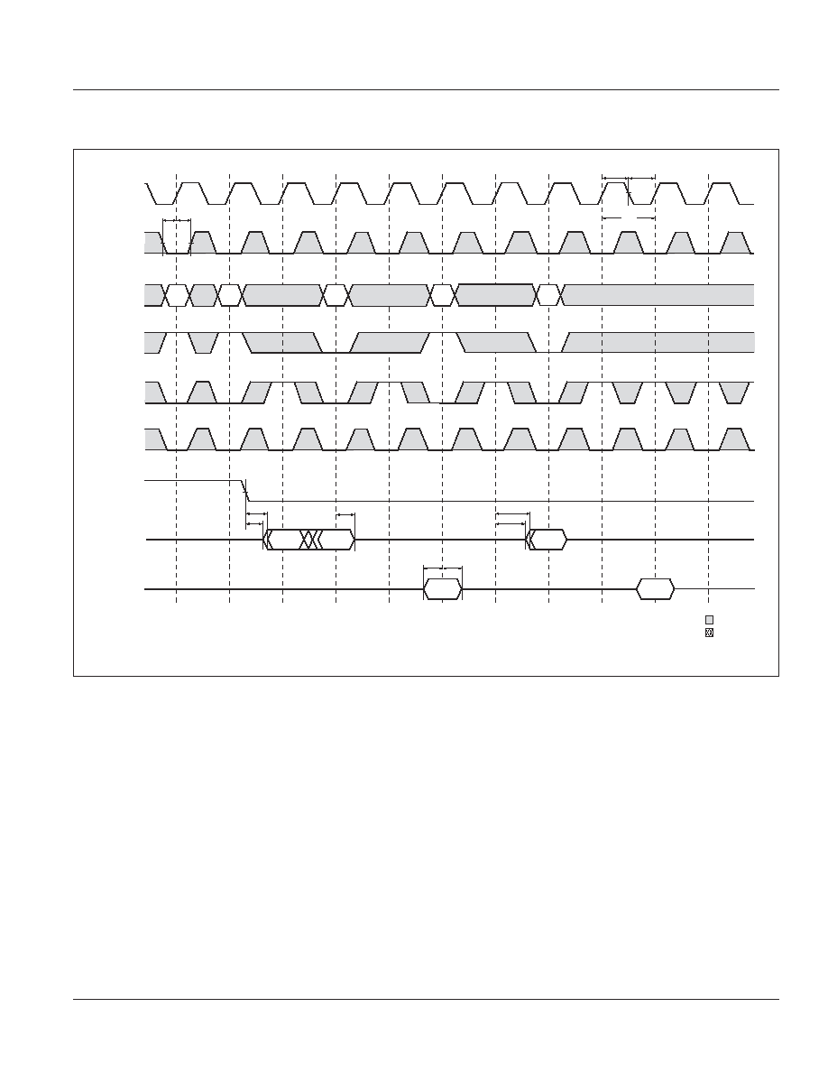
SINGLE READ/WRITE CYCLE TIMING
CLK
CKE
Address
WRITE
CE
ADV
OE
Data Out
Data In
D5
t
SE
t
HE
t
KH
t
KL
t
KC
Don't Care
Undefined
NOTES:
WRITE
= L means
WE
= L and
BW
x = L
CE
= L means
CE
1 = L, CE2 = H and
CE
2 = L
CE
= H means
CE
1 = H, or
CE
1 = L and
CE
2 = H, or
CE
1 = L and CE2 = L
D2
t
OELZ
t
OEQ
A1 A2 A3
A4 A5 A6 A7
A8 A9
Q1 Q3 Q4
Q6
Q7
t
DS
t
DH

22
Integrated Silicon Solution, Inc. -- www.issi.com --
1-800-379-4774
Rev. 00C
09/12/05
ISSI
Æ
IS61NLP12832A
IS61NLP12836A/IS61NVP12836A
IS61NLP25618A/IS61NVP25618A
CKE
CKE
CKE
CKE
CKE
OPERATION TIMING
A1 A2 A3
A4 A5
A6
Q1 Q3
Q4
CLK
CKE
Address
WRITE
CE
ADV
OE
Data Out
Data In
D2
t
SE
t
HE
t
KH
t
KL
t
KC
t
KQLZ
t
KQHZ
t
KQ
t
DH
t
DS
Don't Care
Undefined
NOTES:
WRITE
= L means
WE
= L and
BW
x = L
CE
= L means
CE
1 = L, CE2 = H and
CE
2 = L
CE
= H means
CE
1 = H, or
CE
1 = L and
CE
2 = H, or
CE
1 = L and CE2 = L
Integrated Silicon Solution, Inc. -- www.issi.com --
1-800-379-4774
23
Rev. 00C
09/12/05
ISSI
Æ
IS61NLP12832A
IS61NLP12836A/IS61NVP12836A
IS61NLP25618A/IS61NVP25618A
CE
CE
CE
CE
CE
OPERATION TIMING
Don't Care
Undefined
CLK
CKE
Address
WRITE
CE
ADV
OE
Data Out
Data In
t
SE
t
HE
t
KH
t
KL
t
KC
NOTES:
WRITE
= L means
WE
= L and
BW
x = L
CE
= L means
CE
1 = L, CE2 = H and
CE
2 = L
CE
= H means
CE
1 = H, or
CE
1 = L and
CE
2 = H, or
CE
1 = L and CE2 = L
D5
D3
t
DH
t
DS
t
OELZ
t
OEQ
Q1 Q2
Q4
t
KQHZ
t
KQLZ
t
KQ
A1 A2
A3
A4
A5

24
Integrated Silicon Solution, Inc. -- www.issi.com --
1-800-379-4774
Rev. 00C
09/12/05
ISSI
Æ
IS61NLP12832A
IS61NLP12836A/IS61NVP12836A
IS61NLP25618A/IS61NVP25618A
ORDERING INFORMATION (V
DD
= 3.3V/V
DDQ
= 2.5V/3.3V)
Commercial Range: 0∞C to +70∞C
Access Time
Order Part Number
Package
128Kx32
250
IS61NLP12832A-250TQ
100 TQFP
IS61NLP12832A-250B3
165 PBGA
IS61NLP12832A-250B2
119 PBGA
200
IS61NLP12832A-200TQ
100 TQFP
IS61NLP12832A-200B3
165 PBGA
IS61NLP12832A-200B2
119 PBGA
128Kx36
250
IS61NLP12836A-250TQ
100 TQFP
IS61NLP12836A-250B3
165 PBGA
IS61NLP12836A-250B2
119 PBGA
200
IS61NLP12836A-200TQ
100 TQFP
IS61NLP12836A-200B3
165 PBGA
IS61NLP12836A-200B2
119 PBGA
256Kx18
250
IS61NLP25618A-250TQ
100 TQFP
IS61NLP25618A-250B3
165 PBGA
IS61NLP25618A-250B2
119 PBGA
200
IS61NLP25618A-200TQ
100 TQFP
IS61NLP25618A-200B3
165 PBGA
IS61NLP25618A-200B2
119 PBGA

Integrated Silicon Solution, Inc. -- www.issi.com --
1-800-379-4774
25
Rev. 00C
09/12/05
ISSI
Æ
IS61NLP12832A
IS61NLP12836A/IS61NVP12836A
IS61NLP25618A/IS61NVP25618A
ORDERING INFORMATION (V
DD
= 3.3V/V
DDQ
= 2.5V/3.3V)
Industrial Range: -40∞C to +85∞C
Access Time
Order Part Number
Package
128Kx32
250
IS61NLP12832A-250TQI
100 TQFP
IS61NLP12832A-250B3I
165 PBGA
IS61NLP12832A-250B2I
119 PBGA
200
IS61NLP12832A-200TQI
100 TQFP
IS61NLP12832A-200TQLI
100 TQFP, Lead-free
IS61NLP12832A-200B3I
165 PBGA
IS61NLP12832A-200B2I
119 PBGA
128Kx36
250
IS61NLP12836A-250TQI
100 TQFP
IS61NLP12836A-250B3I
165 PBGA
IS61NLP12836A-250B2I
119 PBGA
200
IS61NLP12836A-200TQI
100 TQFP
IS61NLP12836A-200TQLI
100 TQFP, Lead-free
IS61NLP12836A-200B3I
165 PBGA
IS61NLP12836A-200B2I
119 PBGA
256Kx18
250
IS61NLP25618A-250TQI
100 TQFP
IS61NLP25618A-250B3I
165 PBGA
IS61NLP25618A-250B2I
119 PBGA
200
IS61NLP25618A-200TQI
100 TQFP
IS61NLP25618A-200TQLI
100 TQFP, Lead-free
IS61NLP25618A-200B3I
165 PBGA
IS61NLP25618A-200B2I
119 PBGA

26
Integrated Silicon Solution, Inc. -- www.issi.com --
1-800-379-4774
Rev. 00C
09/12/05
ISSI
Æ
IS61NLP12832A
IS61NLP12836A/IS61NVP12836A
IS61NLP25618A/IS61NVP25618A
ORDERING INFORMATION (V
DD
= 2.5V/V
DDQ
= 2.5V)
Commercial Range: 0∞C to +70∞C
Access Time
Order Part Number
Package
128Kx36
250
IS61NVP12836A-250TQ
100 TQFP
IS61NVP12836A-250B3
165 PBGA
IS61NVP12836A-250B2
119 PBGA
200
IS61NVP12836A-200TQ
100 TQFP
IS61NVP12836A-200B3
165 PBGA
IS61NVP12836A-200B2
119 PBGA
256Kx18
250
IS61NVP25618A-250TQ
100 TQFP
IS61NVP25618A-250B3
165 PBGA
IS61NVP25618A-250B2
119 PBGA
200
IS61NVP25618A-200TQ
100 TQFP
IS61NVP25618A-200B3
165 PBGA
IS61NVP25618A-200B2
119 PBGA
Industrial Range: -40∞C to +85∞C
Access Time
Order Part Number
Package
128Kx36
250
IS61NVP12836A-250TQI
100 TQFP
IS61NVP12836A-250B3I
165 PBGA
IS61NVP12836A-250B2I
119 PBGA
200
IS61NVP12836A-200TQI
100 TQFP
IS61NVP12836A-200B3I
165 PBGA
IS61NVP12836A-200B2I
119 PBGA
256Kx18
250
IS61NVP25618A-250TQI
100 TQFP
IS61NVP25618A-250B3I
165 PBGA
IS61NVP25618A-250B2I
119 PBGA
200
IS61NVP25618A-200TQI
100 TQFP
IS61NVP25618A-200B3I
165 PBGA
IS61NVP25618A-200B2I
119 PBGA

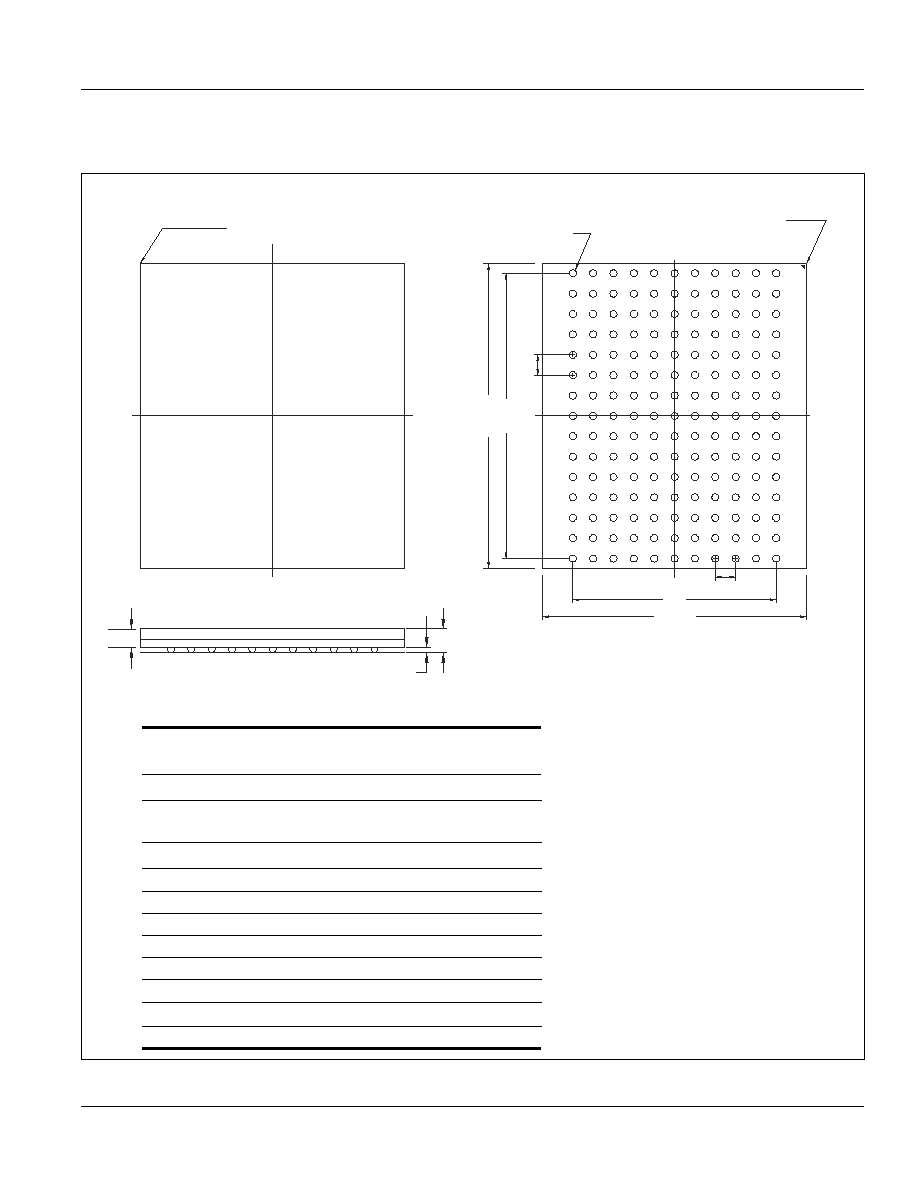
PACKAGING INFORMATION
ISSI
Æ
Integrated Silicon Solution, Inc. -- www.issi.com --
1-800-379-4774
Rev. B
02/12/03
Copyright © 2003 Integrated Silicon Solution, Inc. All rights reserved. ISSI reserves the right to make changes to this specification and its products at any time
without notice. ISSI assumes no liability arising out of the application or use of any information, products or services described herein. Customers are advised to
obtain the latest version of this device specification before relying on any published information and before placing orders for products.
Plastic Ball Grid Array
Package Code: B (119-pin)
Notes:
1. Controlling dimension: millimeters, unless otherwise specified.
2. BSC = Basic lead spacing between centers.
3. Dimensions D1 and E do not include mold flash protrusion and
should be measured from the bottom of the package.
4. Formed leads shall be planar with respect to one another within
0.004 inches at the seating plane.
MILLIMETERS
INCHES
Sym.
Min.
Max.
Min.
Max.
N0.
Leads
119
A
--
2.41
--
0.095
A1
0.50
0.70
0.020
0.028
A2
0.80
1.00
0.032
0.039
A3
1.30
1.70
0.051
0.067
A4
0.56 BSC
0.022 BSC
b
0.60
0.90
0.024
0.035
D
21.80
22.20
0.858
0.874
D1
20.32 BSC
0.800 BSC
D2
19.40
19.60
0.764
0.772
E
13.80
14.20
0.543
0.559
E1
7.62 BSC
0.300 BSC
E2
11.90
12.10
0.469
0.476
e
1.27 BSC
0.050 BSC
E1
A1
D1
7
6
5
4
3
2
1
A
B
C
D
E
F
G
H
J
K
L
M
N
P
R
T
U
E2
E
A2
SEATING PLANE
e
D2
D
A
30
A3
A4
b (119X)
PACKAGING INFORMATION
ISSI
Æ
Integrated Silicon Solution, Inc. -- www.issi.com --
1-800-379-4774
Rev. A
06/11/03
Copyright © 2003 Integrated Silicon Solution, Inc. All rights reserved. ISSI reserves the right to make changes to this specification and its products at any time
without notice. ISSI assumes no liability arising out of the application or use of any information, products or services described herein. Customers are advised to
obtain the latest version of this device specification before relying on any published information and before placing orders for products.
A
B
C
D
E
F
G
H
J
K
L
M
N
P
R
A
B
C
D
E
F
G
H
J
K
L
M
N
P
R
11 10 9 8 7 6 5 4 3 2 1
A1 CORNER
BOTTOM VIEW
D D1
e
e
E1
E
1 2 3 4 5 6 7 8 9 10 11
A1 CORNER
TOP VIEW
A2
A
A1
b (165X)
Ball Grid Array
Package Code: B (165-pin)
Notes:
1. Controlling dimensions are in millimeters.
BGA - 13mm x 15mm
MILLIMETERS
INCHES
Sym.
Min.
Nom.
Max.
Min.
Nom.
Max.
N0.
Leads
165
165
A
--
--
1.20
--
--
0.047
A1
0.25
0.33
0.40
0.010
0.013
0.016
A2
--
0.79
--
--
0.031
--
D
14.90
15.00
15.10
0.587
0.591
0.594
D1
13.90
14.00
14.10
0.547
0.551
0.555
E
12.90
13.00
13.10
0.508
0.512
0.516
E1
9.90
10.00
10.10
0.390
0.394
0.398
e
--
1.00
--
--
0.039
--
b
0.40
0.45
0.50
0.016
0.018
0.020
Integrated Silicon Solution, Inc. -- 1-800-379-4774
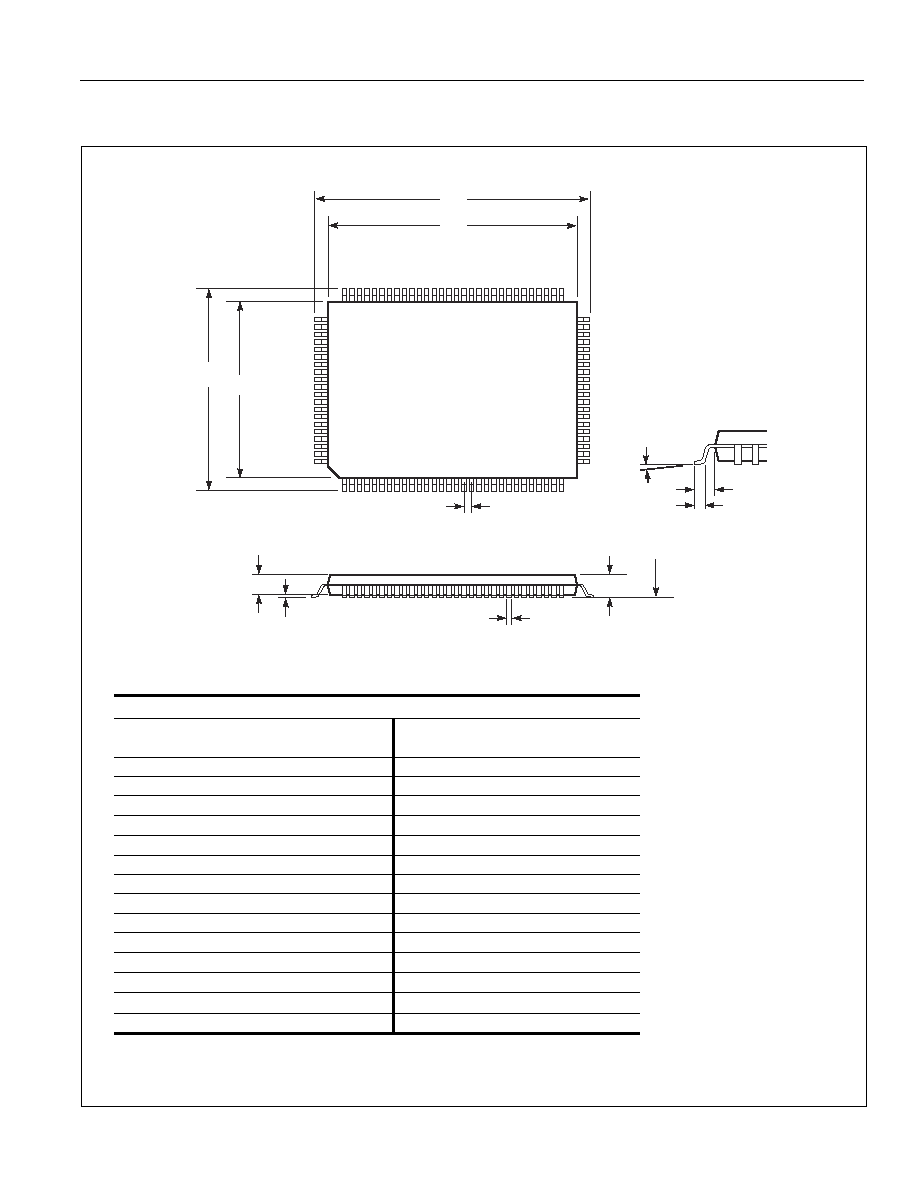
PACKAGING INFORMATION
ISSI
Æ
PK13197LQ Rev. D 05/08/03
TQFP (Thin Quad Flat Pack Package)
Package Code: TQ
Thin Quad Flat Pack (TQ)
Millimeters
Inches
Millimeters
Inches
Symbol
Min
Max
Min
Max
Min
Max
Min
Max
Ref. Std.
No. Leads (N)
100
128
A
--
1.60
--
0.063
--
1.60
--
0.063
A1
0.05
0.15
0.002
0.006
0.05
0.15
0.002
0.006
A2
1.35
1.45
0.053
0.057
1.35
1.45
0.053
0.057
b
0.22
0.38
0.009
0.015
0.17
0.27
0.007
0.011
D
21.90
22.10
0.862
0.870
21.80
22.20
0.858
0.874
D1
19.90
20.10
0.783
0.791
19.90
20.10
0.783
0.791
E
15.90
16.10
0.626
0.634
15.80
16.20
0.622
0.638
E1
13.90
14.10
0.547
0.555
13.90
14.10
0.547
0.555
e
0.65 BSC
0.026 BSC
0.50 BSC
0.020 BSC
L
0.45
0.75
0.018
0.030
0.45
0.75
0.018
0.030
L1
1.00 REF.
0.039 REF.
1.00 REF.
0.039 REF.
C
0
o
7
o
0
o
7
o
0
o
7
o
0
o
7
o
Notes:
1. All dimensioning and
tolerancing conforms to
ANSI Y14.5M-1982.
2. Dimensions D1 and E1 do
not include mold protrusions.
Allowable protrusion is 0.25
mm per side. D1 and E1 do
include mold mismatch and
are determined at datum
plane -H-.
3. Controlling dimension:
millimeters.
D
D1
E
E1
1
N
A2
A
A1
e
b
SEATING
PLANE
C
L1
L