 | –≠–ª–µ–∫—Ç—Ä–æ–Ω–Ω—ã–π –∫–æ–º–ø–æ–Ω–µ–Ω—Ç: 10N100AU1 | –°–∫–∞—á–∞—Ç—å:  PDF PDF  ZIP ZIP |

© 1997 IXYS All rights reserved
TO-247 AD
G
C
E
G = Gate,
C = Collector,
E = Emitter,
TAB = Collector
Symbol
Test Conditions
Maximum Ratings
V
CES
T
J
= 25
∞
C to 150
∞
C
1000
V
V
CGR
T
J
= 25
∞
C to 150
∞
C; R
GE
= 1 M
1000
V
V
GES
Continuous
±
20
V
V
GEM
Transient
±
30
V
I
C25
T
C
= 25
∞
C
20
A
I
C90
T
C
= 90
∞
C
10
A
I
CM
T
C
= 25
∞
C, 1 ms
40
A
SSOA
V
GE
= 15 V, T
VJ
= 125
∞
C, R
G
= 150
I
CM
= 20
A
(RBSOA)
Clamped inductive load, L = 300
µ
H
@ 0.8 V
CES
P
C
T
C
= 25
∞
C
100
W
T
J
-55 ... +150
∞
C
T
JM
150
∞
C
T
stg
-55 ... +150
∞
C
M
d
Mounting torque (M3)
1.13/10 Nm/lb.in.
Weight
6
g
Maximum lead temperature for soldering
300
∞
C
1.6 mm (0.062 in.) from case for 10 s
Symbol
Test Conditions
Characteristic Values
(T
J
= 25
∞
C, unless otherwise specified)
min.
typ.
max.
BV
CES
I
C
= 4 mA, V
GE
= 0 V
1000
V
V
GE(th)
I
C
= 500
µ
A, V
CE
= V
GE
2.5
5.5
V
I
CES
V
CE
= 0.8 ∑ V
CES
T
J
= 25
∞
C
400
µ
A
V
GE
= 0 V
T
J
= 125
∞
C
5
mA
I
GES
V
CE
= 0 V, V
GE
=
±
20 V
±
100
nA
V
CE(sat)
I
C
= I
C90
, V
GE
= 15 V
10N100U1
3.5
V
10N100AU1
4.0
V
V
CES
I
C25
V
CE(sat)
Low V
CE(sat)
IGBT with Diode
IXGH
10
N100U1
1000 V
20 A
3.5 V
High speed IGBT with Diode
IXGH
10
N100AU1
1000 V
20 A
4.0 V
Combi Packs
Features
l
International standard package
JEDEC TO-247 AD
l
IGBT and anti-parallel FRED in one
package
l
2nd generation HDMOS
TM
process
l
Low V
CE(sat)
- for low on-state conduction losses
l
MOS Gate turn-on
- drive simplicity
l
Fast Recovery
Epitaxial Diode (FRED)
- soft recovery with low I
RM
Applications
l
AC motor speed control
l
DC servo and robot drives
l
DC choppers
l
Uninterruptible power supplies (UPS)
l
Switch-mode and resonant-mode
power supplies
Advantages
l
Space savings (two devices in one
package)
l
Easy to mount with 1 screw
(isolated mounting screw hole)
l
Reduces assembly time and cost
91753F (3/97)

IXYS MOSFETS and IGBTs are covered by one or more of the following U.S. patents:
4,835,592
4,881,106
5,017,508
5,049,961
5,187,117
5,486,715
4,850,072
4,931,844
5,034,796
5,063,307
5,237,481
5,381,025
IXYS reserves the right to change limits, test conditions, and dimensions.
IXGH 10N100U1
IXGH 10N100AU1
TO-247 AD Outline
Symbol
Test Conditions
Characteristic Values
(T
J
= 25
∞
C, unless otherwise specified)
min.
typ.
max.
g
fs
I
C
= I
C90
; V
CE
= 10 V,
4
8
S
Pulse test, t
300
µ
s, duty cycle
2 %
C
ies
750
pF
C
oes
V
CE
= 25 V, V
GE
= 0 V, f = 1 MHz
200
pF
C
res
30
pF
Q
g
52
70
nC
Q
ge
I
C
= I
C90
, V
GE
= 15 V, V
CE
= 0.5 V
CES
13
25
nC
Q
gc
24
45
nC
t
d(on)
100
ns
t
ri
200
ns
t
d(off)
550
900
ns
t
fi
10N100U1
800
ns
10N100AU1
500
ns
E
off
10N100AU1
2
3
mJ
t
d(on)
100
ns
t
ri
200
ns
E
on
1.1
mJ
t
d(off)
600
1000
ns
t
fi
10N100U1
1250
2000
ns
10N100AU1
600
1000
ns
E
off
10N100U1
5.0
mJ
10N100AU1
2.5
mJ
R
thJC
1.2 K/W
R
thCK
0.25
K/W
Reverse Diode (FRED)
Characteristic Values
(T
J
= 25
∞
C, unless otherwise specified)
Symbol
Test Conditions
min.
typ.
max.
V
F
I
F
= I
C90
, V
GE
= 0 V,
2.75
V
Pulse test, t
300
µ
s, duty cycle d
2 %
I
RM
I
F
= I
C90
, V
GE
= 0 V, -di
F
/dt = 100 A/
µ
s
6.5
A
t
rr
V
R
= 540 V
T
J
= 125
∞
C
120
ns
I
F
= 1 A; -di/dt = 50 A/
µ
s; V
R
= 30 V T
J
= 25
∞
C
50
60
ns
R
thJC
1.6 K/W
Inductive load, T
J
= 125
∞∞
∞∞
∞
C
I
C
= I
C90
, V
GE
= 15 V, L = 300
µ
H
V
CE
= 0.8 V
CES
, R
G
= R
off
= 150
Remarks: Switching times
may increase
for V
CE
(Clamp) > 0.8 ∑ V
CES
,
higher T
J
or increased R
G
Inductive load, T
J
= 25
∞∞
∞∞
∞
C
I
C
= I
C90
, V
GE
= 15 V, L = 300
µ
H,
V
CE
= 0.8 V
CES
, R
G
= R
off
= 150
Remarks: Switching times
may increase
for V
CE
(Clamp) > 0.8 ∑ V
CES
,
higher T
J
or increased R
G
1 = Gate
2 = Collector
3 = Emitter
Tab = Collector
© 1997 IXYS All rights reserved
IXGH 10N100U1
IXGH 10N100AU1
T
J
- Degrees C
-50
-25
0
25
50
75
100 125 150
B
V
/
V
(t
h
)
-
No
rm
alize
d
0.5
0.6
0.7
0.8
0.9
1.0
1.1
1.2
1.3
T
J
- Degrees C
-50
-25
0
25
50
75
100 125 150
V
(sa
t
)
-
No
rma
lize
d
0.7
0.8
0.9
1.0
1.1
1.2
1.3
1.4
1.5
V
CE
- Volts
0
1
2
3
4
5
I
C
- Am
pe
res
0
2
4
6
8
10
12
14
16
18
20
T
J
= 25∞C
V
GE
= 15V
7V
9V
11V
V
GE
- Volts
5
6
7
8
9
10
11
12
13 14
15
V
CE
-
Vo
lts
0
1
2
3
4
5
6
7
8
9
10
V
GE
- Volts
0
1
2
3
4
5
6
7
8
9
10
I
C
- A
m
p
ere
s
0
2
4
6
8
10
12
14
16
18
20
V
CE
- Volts
0
2
4
6
8
10
12
14
16
18
20
I
C
-
Am
pe
res
0
10
20
30
40
50
60
70
80
13V
11V
9V
7V
13V
T
J
= 25∞C
V
GE
= 15V
I
C
= 5A
I
C
= 10A
I
C
= 20A
V
GE
= 15V
I
C
= 5A
I
C
= 10A
V
CE
= 10V
T
J
= 125∞C
T
J
= 25∞C
T
J
= - 40∞C
V
GE(th)
I
C
= 250µA
BV
CES
I
C
= 3mA
10N100p1.JNB
T
J
= 25∞C
I
C
= 20A
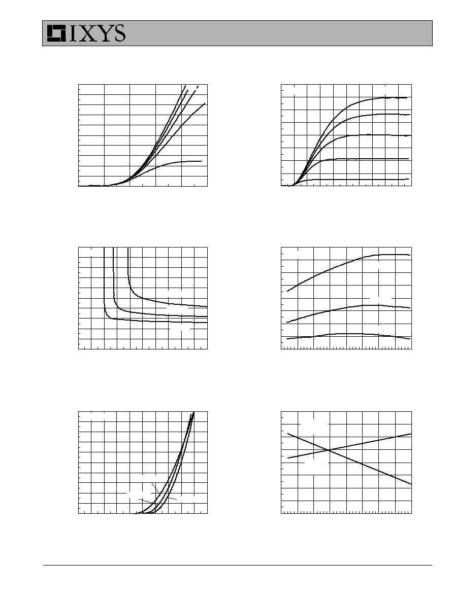
Fig. 3 Collector-Emitter Voltage
Fig. 4 Temperature Dependence
vs. Gate-Emitter Voltage
of Output Saturation Voltage
Fig. 5 Input Admittance
Fig. 6 Temperature Dependence of
Breakdown and Threshold Voltage
Fig. 1 Saturation Characteristics
Fig. 2 Output Characterstics

IXYS MOSFETS and IGBTs are covered by one or more of the following U.S. patents:
4,835,592
4,881,106
5,017,508
5,049,961
5,187,117
5,486,715
4,850,072
4,931,844
5,034,796
5,063,307
5,237,481
5,381,025
IXYS reserves the right to change limits, test conditions, and dimensions.
IXGH 10N100U1
IXGH 10N100AU1
I
C
- Amperes
4
6
8
10
12
14
16
18
20
22
t
fi
- nan
os
eco
nds
600
650
700
750
800
850
900
E
of
f
- m
illij
oule
s
1
2
3
4
5
6
7
R
G
- Ohms
20
40
60
80
100
120
140
160
E
of
f
-
mil
lijou
les
0
1
2
3
4
5
t
fi
- na
no
sec
ond
s
0
200
400
600
800
1000
Time - Seconds
0.00001
0.0001
0.001
0.01
0.1
1
T
h
e
rma
l R
esp
ons
e -
K/W
0.01
0.1
1
V
CE
- Volts
0
200
400
600
800
1000
I
C
-
Am
pe
res
0.01
0.1
1
10
T
J
= 125∞C
R
G
= 150
dV/dt < 3V/ns
Q
g
- nCoulombs
0
10
20
30
40
50
V
GE
- Vol
ts
0
3
6
9
12
15
tfi
Eoff
tfi
Eoff
D=0.1
D=0.2
Single Pulse
D = Duty Cycle
D=0.01
I
C
= 10A
I
C
= 10A
V
CE
= 800V
R
G
=150
TJ =125∞C
T
J
=125∞C
D=0.05
D=0.02
D=0.5
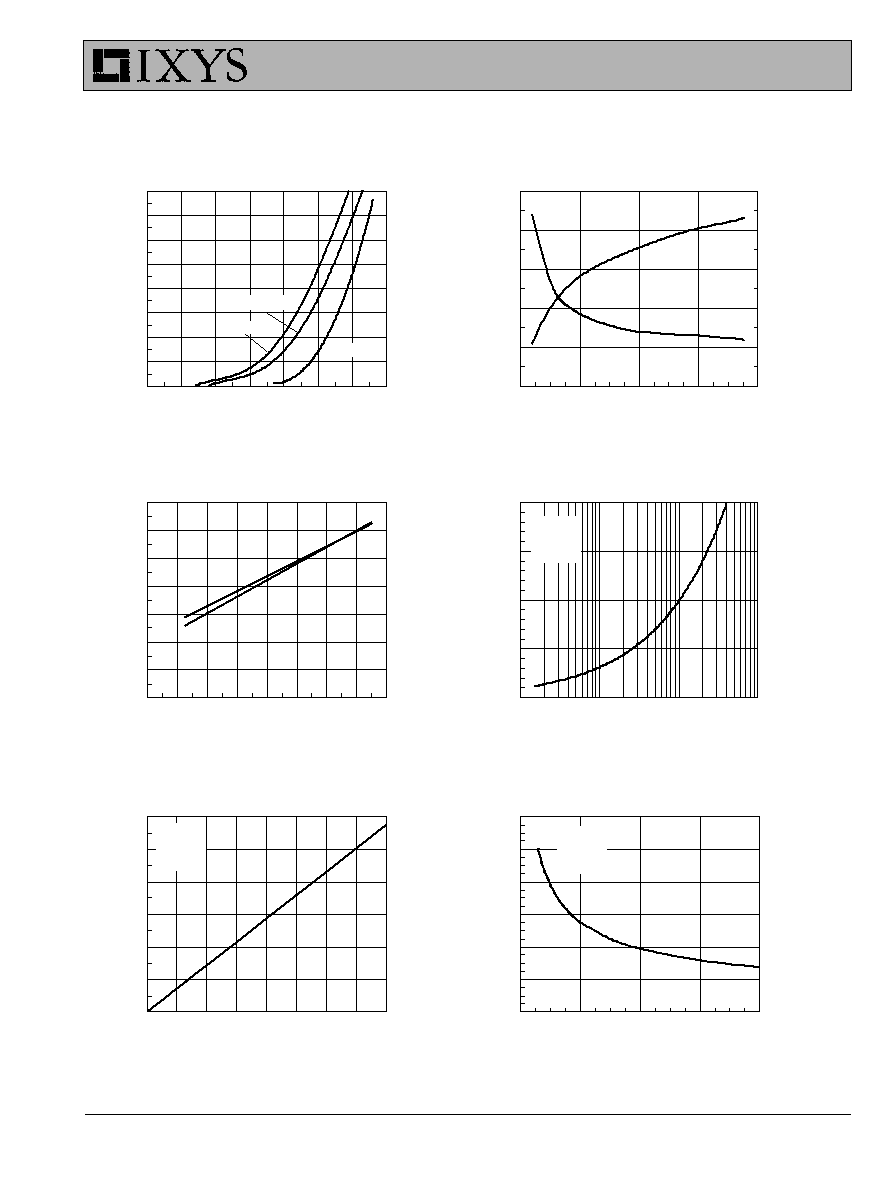
Fig.11 Transient Thermal Impedance
Fig.9 Gate Charge Characteristic Curve Fig.10 Turn-Off Safe Operating Area
Fig.7 Turn-Off Energy per Pulse and Fig.8 Dependence of Turn-Off Energy
Fall Time on Collector Current
Per Pulse and Fall Time on R
G
© 1997 IXYS All rights reserved
IXGH 10N100U1
IXGH 10N100AU1
di
F
/dt - A/µs
0
100
200
300
400
t
rr
-
nano
sec
ond
s
0
100
200
300
400
500
600
di
F
/dt - A/µs
100
200
300
400
I
RM
-
A
m
per
es
0
5
10
15
20
25
30
di
F
/dt - A/µs
1
10
100
1000
Q
r
-
n
anoc
oul
o
m
b
s
0.0
0.5
1.0
1.5
2.0
T
J
- Degrees C
0
20
40
60
80
100
120
140
160
N
o
r
m
a
liz
e
d
I
RM
/Q
r
0.0
0.2
0.4
0.6
0.8
1.0
1.2
1.4
Q
r
I
RM
di
F
/dt - A/µs
0
100
200
300
400
t
fr
-
n
ano
sec
ond
s
0
200
400
600
800
1000
V
FR
- V
o
l
t
s
0
10
20
30
40
50
t
fr
V
FR
T
J
= 125∞C
I
F
= 12A
Voltage Drop - Volts
0.0
0.5
1.0
1.5
2.0
2.5
3.0
3.5
C
u
r
r
e
n
t
- A
m
p
e
re
s
0
5
10
15
20
25
30
35
40
T
J
= 150∞C
T
J
= 100∞C
V
R
= 540V
I
F
= 12A
T
J
= 100∞C
T
J
= 25∞C
T
J
= 100∞C
V
R
= 540V
I
F
= 12A
T
J
= 100∞C
V
R
= 540V
I
F
= 12A
Fig.14 Junction Temperature Dependence Fig.15 Reverse Recovery Chargee
off I
RM
and Q
r
Fig.16 Peak Reverse Recovery Current Fig.17 Reverse Recovery Time
Fig.12 Maximum Forward Voltage Drop Fig.13 Peak Forward Voltage V
FR
and
Forward Recovery Time t
FR