1 - 4
© 2000 IXYS All rights reserved
Symbol
Test Conditions
Maximum Ratings
V
CES
T
J
= 25
∞
C to 150
∞
C
600
V
V
CGR
T
J
= 25
∞
C to 150
∞
C; R
GE
= 1 M
W
600
V
V
GES
Continuous
±
20
V
V
GEM
Transient
±
30
V
I
C25
T
C
= 25
∞
C
60
A
I
C110
T
C
= 110
∞
C
32
A
I
CM
T
C
= 25
∞
C, 1 ms
120
A
SSOA
V
GE
= 15 V, T
VJ
= 125
∞
C, R
G
= 10
W
I
CM
= 64
A
(RBSOA)
Clamped inductive load, L = 100
m
H
@ 0.8 V
CES
P
C
T
C
= 25
∞
C
200
W
T
J
-55 ... +150
∞
C
T
JM
150
∞
C
T
stg
-55 ... +150
∞
C
Maximum lead temperature for soldering
300
∞
C
1.6 mm (0.062 in.) from case for 10 s
M
d
Mounting torque (M3)
1.13/10 Nm/lb.in.
Weight
TO-247 AD
6
g
TO-268
4
g
Symbol
Test Conditions
Characteristic Values
(T
J
= 25
∞
C, unless otherwise specified)
min.
typ.
max.
BV
CES
I
C
= 250
m
A, V
GE
= 0 V
600
V
V
GE(th)
I
C
= 250
m
A, V
CE
= V
GE
2.5
5
V
I
CES
V
CE
= 0.8 ∑ V
CES
T
J
= 25
∞
C
200
m
A
V
GE
= 0 V
T
J
= 150
∞
C
1
mA
I
GES
V
CE
= 0 V, V
GE
=
±
20 V
±
100
nA
V
CE(sat)
I
C
= I
C110
, V
GE
= 15 V
2.1
2.5
V
97538B (7/00)
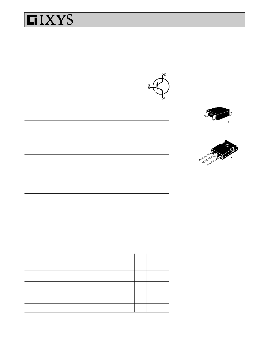
TO-268
(IXGT)
C (TAB)
G = Gate,
C = Collector,
E = Emitter,
TAB = Collector
G
C
E
TO-247 AD
(IXGH)
E
C (TAB)
Features
∑ International standard packages
JEDEC TO-247 and surface
mountable TO-268
∑ High current handling capability
∑ Latest generation HDMOS
TM
process
∑ MOS Gate turn-on
- drive simplicity
Applications
∑ PFC circuits
∑ Uninterruptible power supplies (UPS)
∑ Switched-mode and resonant-mode
power supplies
∑ AC motor speed control
∑ DC servo and robot drives
∑ DC choppers
Advantages
∑ High power density
∑ Very fast switching speeds for high
frequency applications
IXGH 32N60C
V
CES
= 600 V
IXGT 32N60C
I
C25
= 60 A
V
CE(sat)typ
= 2.1 V
t
fi typ
= 55 ns
HiPerFAST
TM
IGBT
Lightspeed
TM
Series
G
IXYS reserves the right to change limits, test conditions, and dimensions.
2 - 4
© 2000 IXYS All rights reserved
Symbol
Test Conditions
Characteristic Values
(T
J
= 25
∞
C, unless otherwise specified)
min.
typ.
max.
g
fs
I
C
= I
C110
; V
CE
= 10 V,
25
S
Pulse test, t
£
300
m
s, duty cycle
£
2 %
C
ies
2700
pF
C
oes
V
CE
= 25 V, V
GE
= 0 V, f = 1 MHz
190
pF
C
res
50
pF
Q
g
110
nC
Q
ge
I
C
= I
C110
, V
GE
= 15 V, V
CE
= 0.5 V
CES
22
nC
Q
gc
40
nC
t
d(on)
25
ns
t
ri
20
ns
t
d(off)
85
ns
t
fi
55
ns
E
off
0.32
mJ
t
d(on)
25
ns
t
ri
25
ns
E
on
0.30
mJ
t
d(off)
110
170
ns
t
fi
105
160
ns
E
off
0.85
1.25
mJ
R
thJC
0.62 K/W
R
thCK
(IXGH32N60C)
0.25
K/W
Inductive load, T
J
= 25
∞
C
I
C
= I
C110
, V
GE
= 15 V, L = 100
m
H,
V
CE
= 0.8 V
CES
, R
G
= R
off
= 4.7
W
Remarks: Switching times may
increase for V
CE
(Clamp) > 0.8 ∑ V
CES
,
higher T
J
or increased R
G
Inductive load, T
J
= 150
∞
C
I
C
= I
C110
, V
GE
= 15 V, L = 100
m
H
V
CE
= 0.8 V
CES
, R
G
= R
off
= 4.7
W
Remarks: Switching times may
increase for V
CE
(Clamp) > 0.8 ∑ V
CES
,
higher T
J
or increased R
G
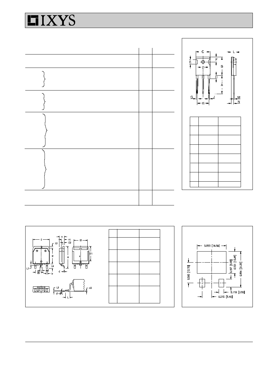
TO-247 AD (IXGH) Outline
Dim. Millimeter
Inches
Min.
Max.
Min.
Max.
A
19.81 20.32
0.780 0.800
B
20.80 21.46
0.819 0.845
C
15.75 16.26
0.610 0.640
D
3.55
3.65
0.140 0.144
E
4.32
5.49
0.170 0.216
F
5.4
6.2
0.212 0.244
G
1.65
2.13
0.065 0.084
H
-
4.5
-
0.177
J
1.0
1.4
0.040 0.055
K
10.8
11.0
0.426 0.433
L
4.7
5.3
0.185 0.209
M
0.4
0.8
0.016 0.031
N
1.5
2.49
0.087 0.102
Dim.
Millimeter
Inches
Min.
Max.
Min.
Max.
A
4.9
5.1
.193
.201
A
1
2.7
2.9
.106
.114
A
2
.02
.25
.001
.010
b
1.15
1.45
.045
.057
b
2
1.9
2.1
.75
.83
C
.4
.65
.016
.026
D
13.80
14.00
.543
.551
E
15.85
16.05
.624
.632
E
1
13.3
13.6
.524
.535
e 5.45 BSC .215 BSC
H
18.70
19.10
.736
.752
L
2.40
2.70
.094
.106
L1
1.20
1.40
.047
.055
L2
1.00
1.15
.039
.045
L3 0.25 BSC .010 BSC
L4
3.80
4.10
.150
.161
TO-268AA (D
3
PAK)
Min. Recommended Footprint
IXGH 32N60C
IXGT 32N60C
IXYS MOSFETS and IGBTs are covered by one or more of the following U.S. patents:
4,835,592
4,881,106
5,017,508
5,049,961
5,187,117
5,486,715
4,850,072
4,931,844
5,034,796
5,063,307
5,237,481
5,381,025
3 - 4
© 2000 IXYS All rights reserved
V
CE
- Volts
0
1
2
3
4
5
I
C
- A
m
p
e
re
s
0
20
40
60
80
100
V
CE
- Volts
0
1
2
3
4
5
I
C
- Am
p
e
re
s
0
20
40
60
80
100
V
CE
-Volts
0
5
10
15
20
25
30
35
40
C
a
p
a
ci
t
a
n
ce -
p
F
10
100
1000
10000
T
J
- Degrees C
25
50
75
100
125
150
V
CE
(
s
a
t
)
- N
o
rm
a
l
iz
e
d
0.50
0.75
1.00
1.25
1.50
V
GE
- Volts
3
4
5
6
7
8
9
10
I
C
- Am
p
e
re
s
0
20
40
60
80
100
V
CE
- Volts
0
2
4
6
8
10
I
C
- Am
p
e
re
s
0
40
80
120
160
200
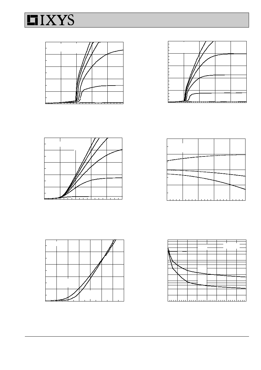
13V
11V
9V
7V
V
CE
= 10V
V
GE
= 15V
13V
T
J
= 25∞C
V
GE
= 15V
T
J
= 25∞C
I
C
= 16A
I
C
= 32A
I
C
= 64A
T
J
=
125∞C
f = 1Mhz
5V
5V
V
GE
= 15V
T
J
= 25∞C
T
J
= 125∞C
7V
9V
5V
7V
9V
V
GE
= 15V
13V
C
iss
C
oss
C
rss
11V
11V
IXGH 32N60C
IXGT 32N60C
Fig. 1. Output Characteristics
Fig. 2. Extended Output Characteristics
Fig. 3. High Temperature Output Characteristics
Fig. 4. Temperature Dependence of V
CE(sat)
Fig. 5. Admittance Curves
Fig. 6. Capacitance Curves

4 - 4
© 2000 IXYS All rights reserved
IXGH 32N60C
IXGT 32N60C
Fig. 7. Dependence of E
ON
and E
OFF
on I
C
.
Fig. 8. Dependence of E
ON
and E
OFF
on R
G
.
Fig. 9. Gate Charge
Fig. 10. Turn-off Safe Operating Area
Fig. 11. Transient Thermal Resistance
Pulse Width - Seconds
0.00001
0.0001
0.001
0.01
0.1
1
Z
thJC
(K
/W)
0.001
0.01
0.1
1
D=0.2
V
CE
- Volts
0
100
200
300
400
500
600
I
C
-
A
m
pe
r
e
s
0.1
1
10
100
Q
g
- nanocoulombs
0
25
50
75
100
125
V
GE
-
V
o
lt
s
0
4
8
12
16
R
G
- Ohms
0
10
20
30
40
50
60
E
(O
FF)
- m
illijoule
s
0
2
4
6
8
E
(O
N
)
- millijou
l
es
0
1
2
3
4
I
C
- Amperes
0
20
40
60
80
E
(O
FF)
- milliJ
oule
s
0
1
2
3
4
E
(O
N
)
- m
illijoule
s
0.00
0.25
0.50
0.75
1.00
V
CE
= 300V
I
C
= 16A
I
C
= 32A
E
(ON)
E
(OFF)
E
(OFF)
T
J
= 125∞C
R
G
= 4.7
dV/dt < 5V/ns
D=0.5
D=0.1
D=0.05
D=0.02
D=0.01
Single pulse
D = Duty Cycle
R
G
= 10
T
J
= 125∞C
64
E
(ON)
I
C
= 64A
E
(OFF)
T
J
= 125∞C
E
(ON)
I
C
= 32A
E
(ON)
E
(OFF)