 | –≠–ª–µ–∫—Ç—Ä–æ–Ω–Ω—ã–π –∫–æ–º–ø–æ–Ω–µ–Ω—Ç: 35N100U1 | –°–∫–∞—á–∞—Ç—å:  PDF PDF  ZIP ZIP |
IXYS Corporation
3540 Bassett Street, Santa Clara CA 95054
Phone: 408-982-0700, Fax: 408-496-0670
IXYS Semiconductor GmbH
Edisonstr. 15, D-68623 Lampertheim
Phone: +49-6206-503-0, Fax: +49-6206-503627
© IXYS Corporation. All rights reserved.
Symbol
Test Conditions
Maximum Ratings
V
CES
T
J
= 25
∞
C to 150
∞
C
1000
V
V
CGR
T
J
= 25
∞
C to 150
∞
C; R
GE
= 1 M
1000
A
V
GES
Continuous
±
20
V
V
GEM
Transient
±
30
V
I
C25
T
C
= 25
∞
C
38
A
I
C90
T
C
= 90
∞
C
25
A
I
CM
T
C
= 25
∞
C, 1 ms
50
A
SSOA
V
GE
= 15 V, T
VJ
= 125
∞
C, R
G
= 22
I
CM
= 50
A
(RBSOA)
Clamped inductive load, L = 30
µ
H
@ 0.8 V
CES
t
SC
V
GE
= 15 V, V
CE
= 0.6 ∑ V
CES
, T
J
= 125
∞
C
10
µ
s
(SCSOA)
R
G
= 22
, non repetitive
P
C
T
C
= 25
∞
C
205
W
V
ISOL
50/60 Hz
t = 1 min
2500
V~
I
ISOL
1 mA
t = 1 s
3000
V~
T
J
-40 ... +150
∞
C
T
JM
150
∞
C
T
stg
-40 ... +150
∞
C
M
d
Mounting torque
1.5/13 Nm/lb.in.
Terminal connection torque (M4)
1.5/13 Nm/lb.in.
Weight
30
g
IGBT with Diode
IXSN 35N100U1
V
CES
= 1000 V
I
C25
= 38 A
V
CE(sat)
= 3.5 V
High Short Circuit SOA Capability
Symbol
Test Conditions
Characteristic Values
(T
J
= 25
∞
C, unless otherwise specified)
min.
typ.
max.
BV
CES
I
C
= 6 mA, V
GE
= 0 V
1000
V
V
GE(th)
I
C
= 10 mA, V
CE
= V
GE
5
8
V
I
CES
V
CE
= 0.8 ∑ V
CES
T
J
= 25
∞
C
750
µ
A
V
GE
= 0 V
T
J
= 125
∞
C
15
mA
I
GES
V
CE
= 0 V, V
GE
=
±
20 V
±
500
nA
V
CE(sat)
I
C
= I
C90
, V
GE
= 15 V
3.5
V
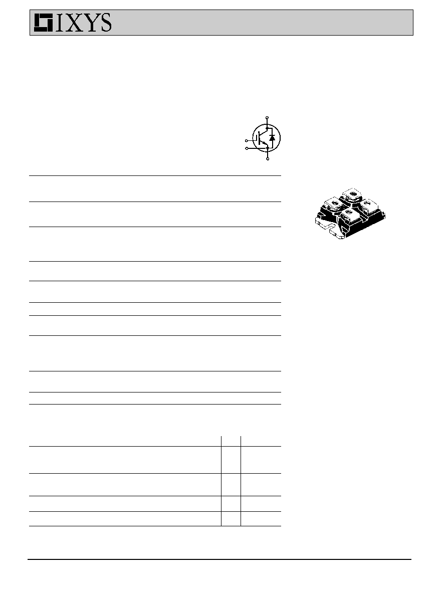
miniBLOC, SOT-227 B
2
1
4
3
1 = Emitter,
3 = Collector
2 = Gate,
4 = Kelvin Emitter
Features
q
International standard package
miniBLOC (ISOTOP) compatible
q
Isolation voltage 3000 V~
q
2nd generation HDMOS
TM
process
- for high short circuit SOA
q
Low V
CE(sat)
- for minimum on-state conduction
losses
q
MOS Gate turn-on
- drive simplicity
q
Fast Recovery
Epitaxial Diode
(FRED)
- short t
rr
and I
RM
q
Low collector-to-case capacitance
(< 50 pF)
- reducesd RFI
q
Low package inductance (< 10 nH)
- easy to drive and to protect
Applications
q
AC motor speed control
q
DC servo and robot drives
q
DC choppers
q
Uninterruptible power supplies (UPS)
q
Switch-mode and resonant-mode
power supplies
Advantages
q
Space savings
q
Easy to mount with 2 screws
q
High power density
2
4
3
1
IXYS reserves the right to change limits, test conditions and dimensions.
93005C (7/94)
IXYS Semiconductor GmbH
Edisonstr. 15, D-68623 Lampertheim
Phone: +49-6206-503-0, Fax: +49-6206-503627
IXYS reserves the right to change limits, test conditions, and dimensions.
IXYS Corporation
3540 Bassett Street, Santa Clara CA 95054
Phone: 408-982-0700, Fax: 408-496-0670
IXSN 35N100U1
Symbol
Test Conditions
Characteristic Values
(T
J
= 25
∞
C, unless otherwise specified)
min.
typ.
max.
g
fs
I
C
= I
C90
; V
CE
= 20 V,
10
20
S
Pulse test, t
300
µ
s, duty cycle d
2 %
I
C(on)
V
GE
= 15 V
300
A
C
ies
4.5
nF
C
oes
V
CE
= 25 V, V
GE
= 0 V, f = 1 MHz
0.5
nF
C
res
0.09
nF
Q
g
180
nC
Q
ge
I
C
= I
C90
, V
GE
= 15 V, V
CE
= 0.5 V
CES
45
nC
Q
gc
120
nC
t
d(on)
80
ns
t
ri
150
ns
t
d(off)
800
ns
t
fi
2000
ns
E
on
3.2
mJ
E
off
6.8
mJ
R
thJC
0.61 K/W
R
thCK
0.05
K/W
Reverse Diode (FRED)
Characteristic Values
(T
J
= 25
∞
C, unless otherwise specified)
Symbol
Test Conditions
min.
typ.
max.
V
F
I
F
= I
C90
, V
GE
= 0 V,
2.3
V
Pulse test, t
300
µ
s, duty cycle d
2 %
I
RM
I
F
= I
C90
, V
GE
= 0 V, -di
F
/dt = 480 A/
µ
s
33
A
t
rr
T
J
= 125
∞
C, V
R
= 360 V
150
ns
R
thJC
0.7 K/W
Inductive load, T
J
= 125
∞∞
∞∞
∞
C
I
C
= I
C90
, V
GE
= 15 V,
V
CE
= 0.6 ∑ V
CES
, R
on
= 6.8
, R
off
= 22
Remarks: Switching times may increase
for V
CE
(Clamp) > 0.6 ∑ V
CES
, higher T
J
or
increased R
G
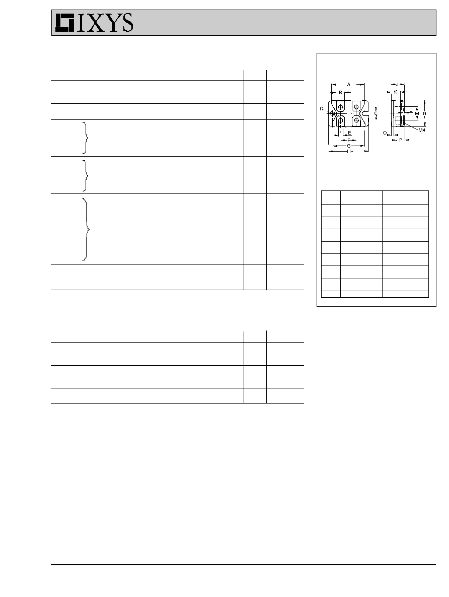
miniBLOC, SOT-227 B
Dim.
Millimeter
Inches
Min.
Max.
Min.
Max.
A
31.5
31.7
1.241
1.249
B
7.8
8.2
0.307
0.323
C
4.0
-
0.158
-
D
4.1
4.3
0.162
0.169
E
4.1
4.3
0.162
0.169
F
14.9
15.1
0.587
0.595
G
30.1
30.3
1.186
1.193
H
38.0
38.2
1.497
1.505
J
11.8
12.2
0.465
0.481
K
8.9
9.1
0.351
0.359
L
0.75
0.85
0.030
0.033
M
12.6
12.8
0.496
0.504
N
25.2
25.4
0.993
1.001
O
1.95
2.05
0.077
0.081
P
-
5.0
-
0.197
M4 screws (4x) supplied
IXYS MOSFETs and IGBTs are covered by one of the following U.S.patents:
4,835,592 4,881,108 5,017,508 5,049,961 5,187,117 5,486,715
4,850,072 4,931,844 5,034,796 5,063,307 5,237,481 5,381,025
IXYS Corporation
3540 Bassett Street, Santa Clara CA 95054
Phone: 408-982-0700, Fax: 408-496-0670
IXYS Semiconductor GmbH
Edisonstr. 15, D-68623 Lampertheim
Phone: +49-6206-503-0, Fax: +49-6206-503627
© IXYS Corporation. All rights reserved.
IXSN 35N100U1
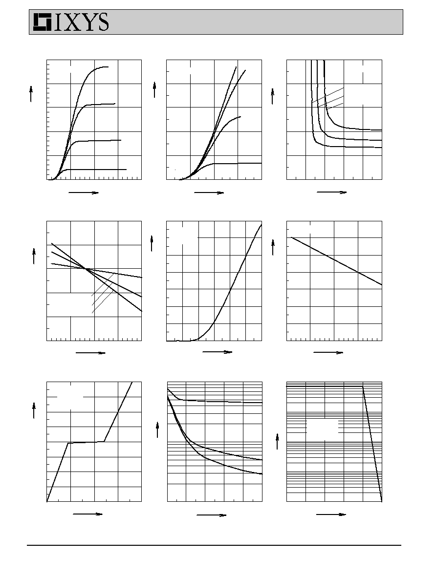
0
200
400
600
800
1000
0.01
0.1
1
10
100
Fig. 9
Reverse biased safe operating area
T
J
= 125∞C
dV/dt < 6 V/ns
R
G
= 22
A
I
C
0
5
10
15
20
25
0.1
1
10
Fig. 8
Typ. capacitances
C
res
C
oes
C
ies
C
nF
0
50
100
150
200
0
2
4
6
8
10
12
14
16
characteristics, V
GE
= f(Q
G
)
Fig. 7
Typ. turn-on gate charge
I
G
= 40 mA
I
C
= 1 A
V
CE
= 25 V
V
-50
0
50
100
150
0.5
0.6
0.7
0.8
0.9
1.0
1.1
1.2
I
C
= 10 mA
Fig. 6
Typ. temp. dependence
of norm.
V
GE(th)
nor m .
V
GE (th )
4
6
8
10
12
14
16
0
50
100
150
200
250
300
350
Fig. 5
Typ. transfer characteristics
V
CE
= 30 V
T
J
= 25∞C
A
I
C
-50
0
50
100
150
0.7
0.8
0.9
1.0
1.1
1.2
Fig. 4
Typ. temp. dependence of V
CE(sat)
I
C
= 12.5 A
I
C
= 50 A
I
C
= 25 A
norm .
∞C
V
CE(sat)
6
8
10
12
14
16
0
2
4
6
8
10
Fig. 3
Typ. on-state characteristics
I
C
= 50 A
I
C
= 25 A
I
C
= 12.5 A
V
0
2
4
6
8
0
30
60
90
120
150
V
CE(sat)
T
J
= 25∞C
9 V
11 V
13 V
15 V
V
CE
A
V
0
5
10
15
20
0
50
100
150
200
250
Fig. 2
Typ. output characteristics
Fig. 1
Typ. output characteristics
T
J
= 25∞C
I
C
T
J
= 25∞C
9 V
11 V
13 V
15 V
A
I
C
V
V
CE
V
GE
V
GE
V
T
J
V
GE
Q
G
V
V
CE
V
CE
V
V
nC
T
J
∞C
IXYS Semiconductor GmbH
Edisonstr. 15, D-68623 Lampertheim
Phone: +49-6206-503-0, Fax: +49-6206-503627
IXYS reserves the right to change limits, test conditions, and dimensions.
IXYS Corporation
3540 Bassett Street, Santa Clara CA 95054
Phone: 408-982-0700, Fax: 408-496-0670
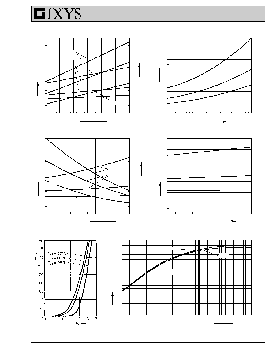
0
10
20
30
40
50
0
2
4
6
8
10
12
14
Fig. 13
Typ. turn-off energy per pulse
I
C
= 12.5 A
I
C
= 50 A
I
C
= 25 A
mJ
R
Goff
E
off
0
10
20
30
40
50
0
2
4
6
8
10
Fig. 12
Typ. turn-on energy per pulse
I
C
= 12.5 A
I
C
= 50 A
12.5
25
37.5
50
65,5
I
C
= 25 A
0
I
RM
A
R
Gon
mJ
E
on
0.0001
0.001
0.01
0.1
1
10
0.01
0.1
1
Fig. 15
Transient thermal resistance junction to case of IGBT and Diode
t
Diode
IGBT
Z
thJC
K/W
s
0
25
50
75
100
125
150
0
2
4
6
8
10
12
14
Fig. 11
Typ. turn-off energy per pulse
I
C
= 50 A
I
C
= 25 A
I
C
= 12.5 A
∞C
mJ
E
off
T
J
0
25
50
75
100
125
150
0
2
4
6
8
10
Fig. 10
Typ. turn-on energy per pulse
I
C
= 50 A
I
C
= 25 A
I
C
= 12.5 A
40
50
A
I
RM
20
0
10
mJ
∞C
T
J
30
E
on
Single pulse
I
RM
I
RM
I
RM
I
RM
I
RM
I
RM
IXSN 35N100U1
Fig. 14
Forward characteristic of
reverse diode

IXYS Corporation
3540 Bassett Street, Santa Clara CA 95054
Phone: 408-982-0700, Fax: 408-496-0670
IXYS Semiconductor GmbH
Edisonstr. 15, D-68623 Lampertheim
Phone: +49-6206-503-0, Fax: +49-6206-503627
© IXYS Corporation. All rights reserved.

IXYS Semiconductor GmbH
Edisonstr. 15, D-68623 Lampertheim
Phone: +49-6206-503-0, Fax: +49-6206-503627
IXYS reserves the right to change limits, test conditions, and dimensions.
IXYS Corporation
3540 Bassett Street, Santa Clara CA 95054
Phone: 408-982-0700, Fax: 408-496-0670