1
IXYS reserves the right to change limits, test conditions and dimensions
Contents
Page
Symbols and Definitions
2
Nomenclature
2
General Information
3
Assembly Instructions
4
FRED, Rectifier Diode and Thyristor Chips in Planar Design
5
IGBT Chips
V
CES
I
C
G-Series, Low V
CE(sat)
B2 Types
600 ...1200 V
7 ... 20 A
6
G-Series, Fast C2 Types
600 V
7 ... 20 A
6
S-Series, SCSOA Capability, Fast Types
600 V
10 ... 20 A
6
E-Series, Improved NPT� technology
1200 ... 1700 V
20 ... 150 A
7
MOSFET Chips
V
DSS
R
DS(on)
HiPerFET
TM
Power MOSFET
70 ...1200 V
0.005 ... 4.5
8-10
PolarHT
TM
MOSFET, very Low R
DS(on)
55 ... 300 V
0.015 ... 0.135
11
P-Channel Power MOSFET
-100 ...-600 V
0.06 ... 1.2
12
N-Channel Depletion Mode MOSFET
500 ...1000 V
30 ... 110
12
Layouts
13-17
Bipolar Chips
V
RRM
/ V
DRM
I
F(AV)M
/ I
T(AV)M
Rectifier Diodes
1200 ... 1800 V
12 ... 416 A
18-19
FREDs
600 ... 1200 V
8 ... 244 A
20-21
Low Leakage FREDs
200 ... 1200 V
9 ... 148 A
22-23
SONIC-FRD
TM
Diodes
600 ... 1800 V
12 ... 150 A
24-25
GaAs Schottky Diodes
100 ... 600 V
3.5 ... 25 A
26-27
Schottky Diodes
8 ... 200 V
28 ... 145 A
28-31
Phase Control Thyristors
800 ... 2200 V
15 ... 540 A
32-33
Fast Rectifier Diodes
1600 ... 1800 V
10 ... 26 A
34
Direct Copper Bonded (DCB), Direct Alu Bonded (DAB) Ceramic Substrates
What is DCB/DAB?
35
DCB Specification
36
Chip-Shortform2004.pmd
26.10.2004, 12:44
1

2
� 2004 IXYS All rights reserved
Symbols and Definitions
C
ies
Input capacitance of IGBT
C
iss
Input capacitance of MOSFET
-di/dt
Rate of decrease of forward current
I
C
DC collector current
I
D
Drain current
I
F
Forward current of diode
I
F(AV)M
Maximum average forward current at specified T
h
I
FSM
Peak one cycle surge forward current
I
GT
Gate trigger current
I
R
Reverse current
I
RM
Maximum peak recovery current
I
T
Forward current of thyristor
I
T(AV)M
Maximum average on-state current of a thyristor
at specified T
h
I
TSM
Maximum surge current of a thyristor
R
DS(on)
Static drain-source on-state resistance
R
thjc
Thermal resistance junction to case
r
T
Slope resistance of a thyristor or diode
(for power loss calculations)
T
case
Case temperature
T
h
Heatsink temperature
t
fi
Current fall time with inductive load
T
j
,
T
(vj)
Junction temperature
T
jm
,
T
(vj)m
Maximum junction temperature
t
rr
Reverse recovery time of a diode
V
CE(sat)
Collector-emitter saturation voltage
V
CES
Maximum collector-emitter voltage
V
DRM
Maximum repetitive forward blocking
voltage of thyristor
V
DSS
Drain-source break-down voltage
V
F
Forward voltage of diode
V
R
Reverse voltage
V
RRM
Maximum peak reverse voltage of thyristor or
diode
V
T
On-state voltage of thyristor
V
T0
Threshold voltage of thyristors or diodes (for
power loss calculation only)
Chip and DCB Ceramic Substrates Data book
Edition 2004
Published by IXYS Semiconductor GmbH
Marketing Communications
Edisonstra�e 15, D-68623 Lampertheim
� IXYS Semiconductor GmbH All Rights reserved
As far as patents or other rights of third parties are concerned, liability is only
assumed for chips and DCB parts per se, not for applications, processes and
circuits implemented with components or assemblies. Terms of delivery and the
right to change design or specifications are reserved.
Nomenclature
IGBT and MOSFET Discrete
IXSD 40N60A
(Example)
IX
IXYS
Die technology
E
NPT
3
IGBT
F
HiPerFETTM Power MOSFET
G
Fast IGBT
S
IGBT with SCSOA capability
T
Standard Power MOSFET
D
Unassembled chip (die)
40
Current rating, 40 = 40 A
N
N-channel type
P
P-channel type
60
Voltage class, 60 = 600 V
xx
MOSFET
A
Prime RDS(on) for standard MOSFET
Q
Low gate charge die
Q2
Low gate charge die, 2nd generation
P
PolarHTTM Power MOSFET
L
Linear Mode MOSFET
IGBT
--
No letter, low VCE(sat)
A
Or A2, std speed type
B
Or B2, high speed type
C
Or C2, very high speed type
W-CWP 55-12/18
(Thyristor Example)
W
Package type
C
Chip function
C = Silicon phase control thyristor
W
Unassembled chip
P
Process designator
P = Planar passivated chip
cathode on top
55
Current rating value of one chip in A
12/18
Voltage class, 12/18 = 1200 up to 1800 V
Diode and Thyristor Chips
C-DWEP 69-12
(Diode Example)
C
Package type
D
Chip function
D = Silicon rectifier diode
W
Unassembled chip
EP
Process designator
EP = Epitaxial rectifier diode
N = Rectifier diode, cathode on top
P = Rectifier diode, anode on top
FN = Fast Rectifier diode, cathode on top
FP = Fast Rectifier diode, anode on top
69
Current rating value of one chip in A
-12
Voltage class, 12 = 1200 V
Registration No.:
001947 TS2/765/17557
Registration No.:
001947
Chip-Shortform2004.pmd
26.10.2004, 12:44
2

3
IXYS reserves the right to change limits, test conditions and dimensions
General Informations for Chips
When mounting Power Semiconductor chips to a header, ceramic substrate or hybrid thick film circuit, the solder system and the chip
attach process are very important to the reliability and performance of the final product. This brochure provides several guidelines
that describe recommended chip attachment pro-cedures. These methods have been used successfully for many years at IXYS.
Available forms of chip packings
IXYS offers various options.
Please order from one of the following possibilities:
Packaging Options
Delivery form
C-...*
Chips in tray (Waffle Pack);
Electrically tested
T-...*
Chips in wafer, unsawed;
Bipolar = 5" (125 mm
) wafer; Electrically tested, rejects are inked
W-...*
Chips in wafer on foil, sawed;
Bipolar = 5" (125 mm
) wafer; Electrically tested, rejects are inked
...* must be amended by the exact chip type designation.
Packing, Storage and Handling
Chips should be transported in their original containers. All chip transfer to other containers or for assembly should be done only with
rubber-tipped vacuum pencils. Contact with human skin (or with a tool that has been touched by hand) leaves an oily residue that may
adversely impact subsequent chip attach or reliability.
At temperatures below 104
�F (40�C), there is no limitation on storage time for chips in sealed original packages. Chips removed from
original packages should be assembled immediately. The wetting ability of the contact metallization with solder can be preserved by
storage in a clean and dry nitrogen atmosphere.
The IGBT and MOSFET Chips are electrostatic discharge (ESD) sensitive. Normal ESD precautions for handling must be observed.
Prior to chip attach, all testing and handling of the chips must be done at ESD safe work stations according to DIN IEC 47(CO) 701.
Ionized air blowers are recommended for added ESD protection.
Contamination of the chips degrades the assembly results.Finger prints, dust or oily deposits on the surface of the chips have to be
absolutely avoided.
Rough mechanical treatment can cause damage to the chip.
Electrical Tests
The electrical properties listed in the data sheet presume correctly assembled chips. Testing of non-assembled chips requires the
following precautions:
- High currents have to be supplied homogeneously to the whole metallized contact area.
- Kelvin probes must be used to test voltages at high currents
- Applying the full specified blocking or reverse voltage may cause arcing across the glass passivated junction termination, because
the electrical field on top of the passivation glass causes ionization of the surrounding air. This phenomenon can be avoided by using
inert fluids or by increasing the pressure of the gas surrounding the chip to values above 30 psig (2 bars).
General Rules for Assembly
The linear thermal expansion coefficient of silicon is very small compared to usual contact metals. If a large area metallized silicon
chip is directly soldered to a metal like copper, enormous shear stress is caused by temperature changes (e.g. when cooling down from
the solder temperature or by heating during working conditions) which can disrupt the solder mountdown.
If it is found that larger chips are cracking during mountdown or in the application, then the use of a low thermal expansion coefficient
buffer layer,
e.g. tungsten,
molybdenum or Trimetal
�
, for strain relief should be considered. An alternative solution is to soft-solder these
larger chips to DCB ceramic substrates because of their matching thermal expansion coefficients.
Chip-Shortform2004.pmd
26.10.2004, 12:44
3

4
� 2004 IXYS All rights reserved
MOS/IGBT Chips
Recommended Solder System
IXYS recommends a soft solder chip attach using a solder composition of 92.5 % Pb, 5 % Sn and 2.5 % Ag. The maximum chip attach
temperature is 460�C for MOSFET and 360�C for HiPerFET
TM
and IGBT.
Wire Bonding
It is recommended to use wire of diameter not greater than 0.38 mm (0.015") for bonding to the source emitter and gate pads. Multiple
wires should be used in place of thicker wire to handle high drain or emitter currents. See tables for number of recommended wire
bonds. At smaller gate pads 0.15 mm is recommended.
Thermal Response Testing
To assure good chip attach processing, thermal response testing per MIL STD 750, Method 3161 or equivalent should be performed.
Bipolar Chips
Assembling
IXYS bipolar semiconductor chips have a soft-solderable, multi-layer metallization (Ti/Ni/Ag) on the bottom side and, on top, either
the same metallization scheme or an alumunium layer sufficiently thick for ultrasonic bonding. Note that the last layer of metal for
soldering is pure silver.
Regardless of their type all chips possess the same glass passivated junction termination system on top of the chip. For that reason
they can be easily chip bonded or they can all be simply soldered to a flat contacting electrode in accordance to the General Rules on
Page 3. All kinds of the usual soft solders with melting points below 660�F (350�C) can be used thanks to their pure silver top metal.
Solders with high melting points are preferable due to their better power cycling capability, i.e. they are more resistant to thermal
fatigue.
Soldering temperature should not exceed 750�F (400�C). The maximum temperature should not be applied for more than five
minutes.
As already mentioned above the electrical properties quoted in the data sheets can only be obtained with properly assembled chips.
This is only possible when all contact materials to be soldered together are well wetted and the solder is practically free of voids.
A simple means to achieve good solder connections is to use a belt furnace running with a process gas containing at least 10 %
Hydrogen in Nitrogen.
Other approved methods are also allowed, provided that the above mentioned temperature-time-limits are not exceeded and
temperature shocks above 930�F/min (500 K/min) are avoided.
We do not recommend the use of fluxes for soldering!
Ultrasonic Wire Bonding
Chips provided with a thick aluminium layer are designed for ultrasonic wire bonding. Wire diameters up to 500 �m can be used
dependent on chip types. Setting wires in parallel and application of stitch bonding lead to surge current ratings comparable to
soldered chips.
Coating
Although the chips are glass passivated, they must be protected against arcing and environmental influences. The coating material
that is in contact with the chip surface must have the following properties:
- elasticity (to prevent mechanical stress)
- high purity, no contamination with alkali metals
- good adhesion to metals and glass passivation.
Assembly Instructions
Chip-Shortform2004.pmd
26.10.2004, 12:44
4
5
IXYS reserves the right to change limits, test conditions and dimensions
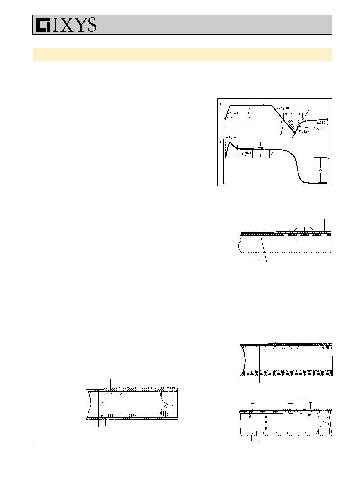
FRED, Rectifier Diode and Thyristor Chips in Planar Design
Fast Recovery Epitaxial Diodes (FRED)
Power switches (IGBT, MOSFET, BJT, GTO) for applications in electronics are only as good as their associated free-wheeling
diodes. At increasing switching frequencies, the proper functioning and efficiency of the power switch, aside from conduction losses,
is determined by the turn-off behavior of the diode (characterized by Q
rr
, I
RM
and t
rr
- Fig. 1.
Rectifier Diode and Thyristor Chips
The figures 3 a-c show cross sectional views of the diode and thyristor
chips in the passivation area. All thyristor and diode chips (DWN, DWFN,
CWP) are fabricated using separation diffusion processes so that all
junctions terminate on the topside of the chip. Now the entire bottom
surfaces of all chips are available for soldering onto a DCB or other ceramic
substrate without a molybdenum strain buffer. The elimination of the strain
buffer and its solder joint reduces thermal resistance and increases
blocking voltage stability. The junction termination areas are passivated
with glass, whose thermal expansion coefficient matches that of silicon. All
silicon chips increasingly use planar technology with guard rings and
channel stoppers to reduce electric fields on the chip surface.
The contact areas of the chips have vapor deposited metal layers which
contribute substantially to their high power cycle capability. All chips are
processed on silicon wafers of 5" diameter and diced after a wafer sample
test which auto-matically marks chips not meeting the electrical specification.
The chip geometry is square or rectangular.
Fig. 3a-c
Cross sections of Chips in the passivation area
a) Diode chip, type DWN, DWFN
b) Diode chip, type DWP, DWFP
c) Thyristor chip, type CWP
The reverse current character-istic following the peak reverse current I
RM
is
another very im-portant property. The slope of the decaying reverse current
di
rr
/dt results from design para- meters (technology and dif-fusion of the
FRED chip Fig. 2. In a circuit this current slope, in conjunction with parasitic
induc-tances (e.g. connecting leads, causes over-voltage spikes and high
frequency interference vol-tages.The higher the di
rr
/dt ("hard recovery" or
"snap-off" behavior) the higher is the resulting additional stress for both the
diode and the paralleled switch. A slow decay of the reverse current ("soft
recovery" behavior), is the most desirable characteristic, and this is designed
into all FRED. The wide range of available blocking voltages makes
it
possible to
apply
these FRED as output rectifiers in switch-mode power
supplies (SMPS) as well as protective and free-wheeling diodes for power
switches in inverters and welding power supplies.
Metalization
Fig. 1: Current and voltage during turn-on and
turn-off switching of fast diodes
Fig. 2: Cross section of glassivated planar epitaxial
diode chip with seperation diffusion (type DWEP)
E pitax ie S ch ich t n -
S ub stra t n+
K atho de
A no de
Guard ring
Substrate n+
Epitaxy layer n-
Cathode
Anode
Glasspassivation
p
n
n
+
Glasspassivation
Guard ring
Metalization
Fig. 3b)
Metalization
Channel-
stopper
Glasspassivation
Guard ring
Emitter
Fig. 3c)
Glasspassivation
Metalization
Fig. 3a)
Chip-Shortform2004.pmd
26.10.2004, 12:44
5