
© 2001 IXYS All rights reserved
1 - 2
DGSK 20-022AS
DGSK 20-025AS
V
RSM
V
RRM
Type
V
V
220
220
DGSK 20-022AS
250
250
DGSK 20-025AS
Preliminary Data
11
9
Symbol
Conditions
Maximum Ratings
I
FAV
T
C
= 25
∞
C; DC
12
A
I
FAV
T
C
= 90
∞
C; DC
9
A
I
FSM
T
VJ
= 45∞C; t
p
= 10 ms (50 Hz), sine
20
A
T
VJ
-55...+175
∞
C
T
stg
-55...+150
∞
C
P
tot
T
C
= 25
∞
C
34
W
Features
q
Low forward voltage
q
Very high switching speed
q
Low junction capacity of GaAs
- low reverse current peak at turn off
q
Soft turn off
q
Temperature independent switching
behaviour
q
High temperature operation capability
q
Epoxy meets UL 94V-0
Applications
q
MHz Switched mode power supplies
(SMPs)
q
Small size SMPs
q
High frequency converters
q
Resonant converters
Pulse test:
Pulse Width = 5 ms, Duty Cycle < 2.0 %
Data according to IEC 60747 and per diode unless otherwise specified
IXYS reserves the right to change limits, Conditions and dimensions.
Gallium Arsenide Schottky Rectifier
I
FAV
= 2x12 A
V
RRM
= 220/250 V
C
Junction
= 18 pF
Symbol
Conditions
Characteristic Values
typ.
max.
I
R
T
VJ
= 25∞C V
R
= V
RRM
1.3
mA
T
VJ
= 125∞C V
R
= V
RRM
1.3
mA
V
F
I
F
= 5 A;
T
VJ
= 125∞C
1.3
V
I
F
= 5 A;
T
VJ
= 25∞C
1.2
1.5
V
C
J
V
R
= 100 V; T
VJ
= 125∞C
18
pF
R
thJC
4.4
K/W
Weight
2
g
A
C
A
A = Anode, C = Cathode
TO-263 AB
A
A
C (TAB)
© 2001 IXYS All rights reserved
2 - 2
DGSK 20-022AS
DGSK 20-025AS
0.0
0.5
1.0
1.5
2.0
0.01
0.1
1
10
0.00001
0.0001
0.001
0.01
0.1
1
10
0.01
0.1
1
10
t
s
K/W
0.1
1
10
100
1000
10
100
C
J
I
F
A
V
F
V
R
V
pF
V
Z
thJC
T
VJ
=
125∞C
25∞C
DGS10-015/018BS
T
VJ
= 125∞C
200
20
Single Pulse
11
9
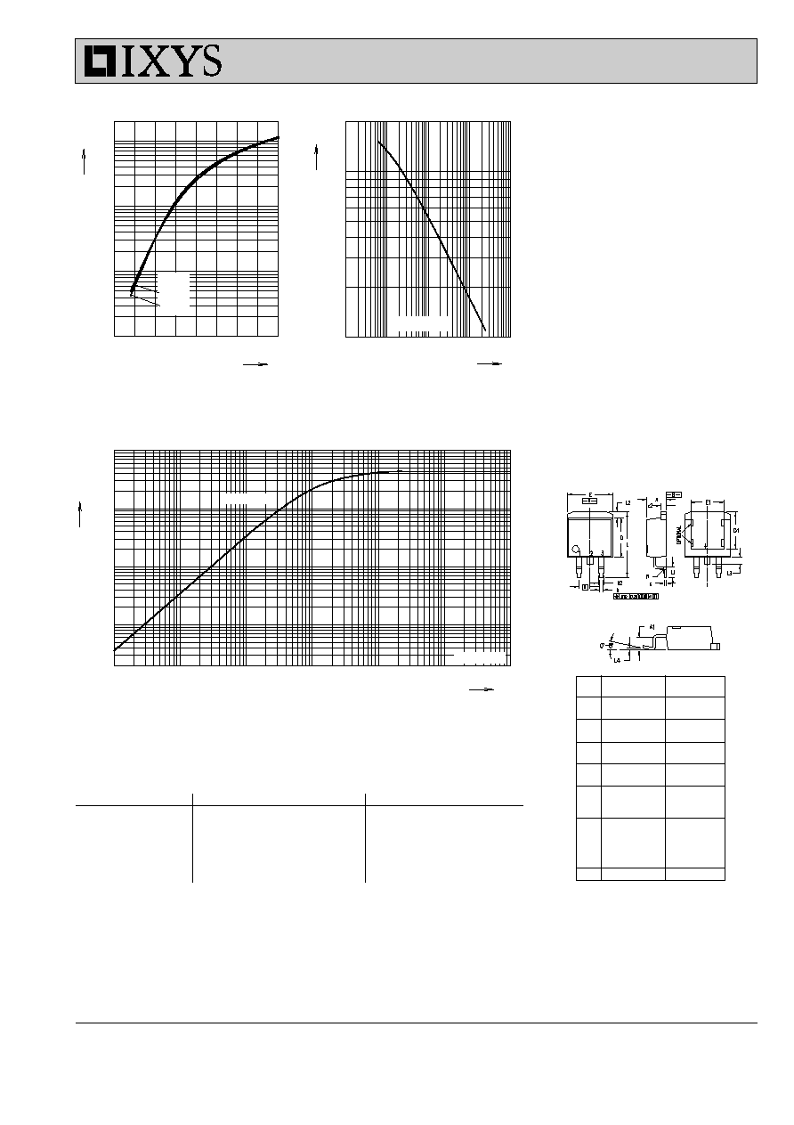
Fig. 1 typ. forward characteristics
Fig. 2 typ. junction capacity
versus blocking voltage
Fig. 3 typ. thermal impedance junction to case
Note:
explanatory comparison of the basic operational behaviour of rectifier diodes and Gallium Arsenide
Schottky diodes:
conduction
forward characteristics
turn off characteristics
turn on characteristics
by majority + minority carriers
V
F
(I
F
)
extraction of excess carriers
causes temperature dependant
reverse recovery (t
rr
, I
RM
, Q
rr
)
delayed saturation leads to V
FR
Rectifier Diode
by majority carriers only
V
F
(I
F
), see Fig. 1
reverse current charges
junction capacity C
J
, see Fig. 2;
not temperature dependant
no turn on overvoltage peak
GaAs Schottky Diode
Outline TO-263 AB
Dim.
Millimeter
Inches
Min.
Max.
Min.
Max.
A
4.06
4.83
.160
.190
A1
2.03
2.79
.080
.110
b
0.51
0.99
.020
.039
b2
1.14
1.40
.045
.055
c
0.46
0.74
.018
.029
c2
1.14
1.40
.045
.055
D
8.64
9.65
.340
.380
D1
8.00
8.89
.315
.350
E
9.65
10.29
.380
.405
E1
6.22
8.13
.245
.320
e 2.54 BSC
.100 BSC
L
14.61
15.88
.575
.625
L1
2.29
2.79
.090
.110
L2
1.02
1.40
.040
.055
L3
1.27
1.78
.050
.070
L4
0
0.20
0
.008
R
0.46
0.74
.018
.029