© 2004 IXYS All rights reserved
1 - 2
DGS 4-025A
DGS 3-025AS
DGSK 8-025A
435
IXYS reserves the right to change limits, test conditions and dimensions
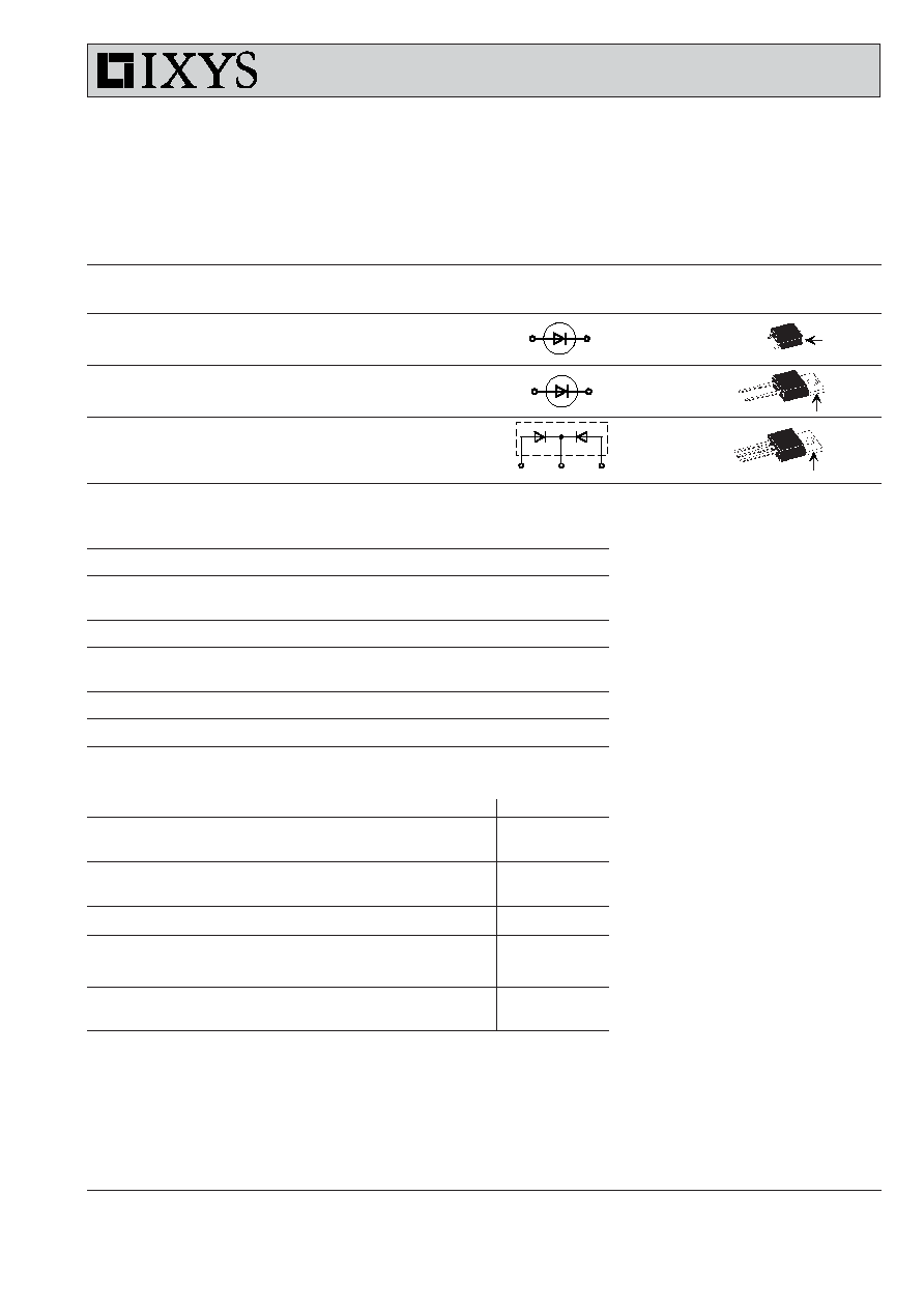
Type
Marking on product
Circuit
Package
DGS 3-025AS
3A250AS
DGS 4-025A
DGS 4-025A
DGSK 8-025A
DGSK 8-025A
Single
Common cathode
Features
∑ Low forward voltage
∑ Very high switching speed
∑ Low junction capacity of GaAs
- low reverse current peak at turn off
∑ Soft turn off
∑ Temperature independent switching
behaviour
∑ High temperature operation capability
∑ Epoxy meets UL 94V-0
Applications
∑ MHz switched mode power supplies
(SMPs)
∑ Small size SMPs
∑ High frequency converters
∑ Resonant converters
Gallium Arsenide Schottky Rectifier
I
FAV
= 5.4 A
V
RRM
= 250 V
C
Junction
= 6.4 pF
A
C
A
C
A
Symbol
Conditions
Maximum Ratings
V
RRM/RSM
250
V
I
FAV
T
C
= 25
∞C; DC
5.4
A
I
FAV
T
C
= 90
∞C; DC
3.9
A
I
FSM
T
VJ
= 45∞C; t
p
= 10 ms (50 Hz), sine
10
A
T
VJ
-55...+175
∞C
T
stg
-55...+150
∞C
P
tot
T
C
= 25
∞C
18
W
M
d
mounting torque (TO-220)
0.4...0.6
Nm
A = Anode, C = Cathode , TAB = Cathode
TO-220 AB
A
C
A
C (TAB)
C
TO-220 AC
A
C (TAB)
A
C
Single
A
TO-252 AA
A
C (TAB)
Pulse test:
Pulse Width = 5 ms, Duty Cycle < 2.0 %
Data according to IEC 60747 and per diode unless otherwise specified
Symbol
Conditions
Characteristic Values
typ.
max.
I
R
T
VJ
= 25∞C V
R
= V
RRM
0.7
mA
T
VJ
= 125∞C V
R
= V
RRM
0.7
mA
V
F
I
F
= 2 A;
T
VJ
= 125∞C
1.3
V
I
F
= 2 A;
T
VJ
= 25∞C
1.3
1.6
V
C
J
V
R
= 100 V; T
VJ
= 125∞C
6.4
pF
R
thJC
8.5
K/W
R
thCH
TO-220
0.5
K/W
Weight
TO-252
0.3
g
TO-220
2
g
© 2004 IXYS All rights reserved
2 - 2
DGS 4-025A
DGS 3-025AS
DGSK 8-025A
435
IXYS reserves the right to change limits, test conditions and dimensions
0,0
0,5
1,0
1,5
2,0
0,001
0,01
0,1
1
10
0,00001
0,0001
0,001
0,01
0,1
1
10
0,01
0,1
1
10
t
s
K/W
0,1
1
10
100
1000
1
10
100
C
J
I
F
A
V
F
V
R
V
pF
V
Z
thJC
T
VJ
= 125∞C
Single Pulse
T
VJ
=
125∞C
25∞C
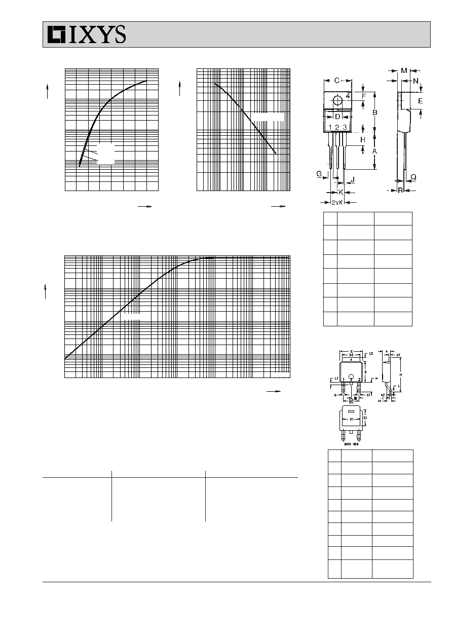
DGS3-025AS
Fig. 1 typ. forward characteristics
Fig. 2 typ. junction capacity
versus blocking voltage
Fig. 3 typ. thermal impedance junction to case
Note:
explanatory comparison of the basic operational behaviour of rectifier diodes and Gallium Arsenide
Schottky diodes:
conduction
forward characteristics
turn off characteristics
turn on characteristics
by majority + minority carriers
V
F
(I
F
)
extraction of excess carriers
causes temperature dependant
reverse recovery (t
rr
, I
RM
, Q
rr
)
delayed saturation leads to V
FR
Rectifier Diode
by majority carriers only
V
F
(I
F
), see Fig. 1
reverse current charges
junction capacity C
J
, see Fig. 2;
not temperature dependant
no turn on overvoltage peak
GaAs Schottky Diode
Outlines
TO-252
1 Anode
2 NC
3 Anode
4 Cathode
Dim. Millimeter
Inches
Min.
Max.
Min.
Max.
A
2.19
2.38
0.086
0.094
A1
0.89
1.14
0.035
0.045
A2
0
0.13
0
0.005
b
0.64
0.89
0.025
0.035
b1
0.76
1.14
0.030
0.045
b2
5.21
5.46
0.205
0.215
c
0.46
0.58
0.018
0.023
c1
0.46
0.58
0.018
0.023
D
5.97
6.22
0.235
0.245
D1
4.32
5.21
0.170
0.205
E
6.35
6.73
0.250
0.265
E1
4.32
5.21
0.170
0.205
e
2.28 BSC
0.090 BSC
e1
4.57 BSC
0.180 BSC
H
9.40 10.42
0.370
0.410
L
0.51
1.02
0.020
0.040
L1
0.64
1.02
0.025
0.040
L2
0.89
1.27
0.035
0.050
L3
2.54
2.92
0.100
0.115
Outline TO-220
Dim.
Millimeter
Inches
Min.
Max.
Min.
Max.
A
12.70
13.97
0.500
0.550
B
14.73
16.00
0.580
0.630
C
9.91
10.66
0.390
0.420
D
3.54
4.08
0.139
0.161
E
5.85
6.85
0.230
0.270
F
2.54
3.18
0.100
0.125
G
1.15
1.65
0.045
0.065
H
2.79
5.84
0.110
0.230
J
0.64
1.01
0.025
0.040
K
2.54
BSC
0.100
BSC
M
4.32
4.82
0.170
0.190
N
1.14
1.39
0.045
0.055
Q
0.38
0.56
0.015
0.022
R
2.29
2.79
0.090
0.110