
© 2000 IXYS All rights reserved
1 - 2
V
RSM
V
RRM
Type
V
V
1200
1200
DSEI 120-12A
Symbol
Test Conditions
Maximum Ratings
I
FRMS
T
VJ
= T
VJM
100
A
I
FAVM
ˇˇx
T
C
= 60
∞
C; rectangular, d = 0.5
109
A
I
FAV
y
T
C
= 95
∞
C; rectangular, d = 0.5
75
A
I
FRM
t
P
< 10
m
s; rep. rating, pulse width limited by T
VJM
tbd
A
I
FSM
T
VJ
= 45
∞
C;
t = 10 ms (50 Hz), sine
600
A
t = 8.3 ms (60 Hz), sine
660
A
T
VJ
= 150
∞
C; t = 10 ms (50 Hz), sine
540
A
t = 8.3 ms (60 Hz), sine
600
A
I
2
t
T
VJ
= 45
∞
C
t = 10 ms (50 Hz), sine
1800
A
2
s
t = 8.3 ms (60 Hz), sine
1800
A
2
s
T
VJ
= 150
∞
C; t = 10 ms (50 Hz), sine
1450
A
2
s
t = 8.3 ms (60 Hz), sine
1500
A
2
s
T
VJ
-40...+150
∞
C
T
VJM
150
∞
C
T
stg
-40...+150
∞
C
P
tot
T
C
= 25
∞
C
357
W
M
d
Mounting torque
0.8...1.2
Nm
Weight
6
g
Symbol
Test Conditions
Characteristic Values
typ.
max.
I
R
T
VJ
= 25
∞
C
V
R
= V
RRM
3
mA
T
VJ
= 25
∞
C
V
R
= 0.8 ∑ V
RRM
1.5
mA
T
VJ
= 125
∞
C
V
R
= 0.8 ∑ V
RRM
20
mA
V
F
I
F
= 70 A;
T
VJ
= 150
∞
C
1.55
V
T
VJ
= 25
∞
C
1.8
V
V
T0
For power-loss calculations only
1.2
V
r
T
T
VJ
= T
VJM
4.6
m
W
R
thJC
0.35
K/W
R
thCK
0.25
K/W
R
thJA
35
K/W
t
rr
I
F
= 1 A; -di/dt = 200 A/
m
s; V
R
= 30 V; T
VJ
= 25
∞
C
40
60
ns
I
RM
V
R
= 350 V;
I
F
= 75 A; -di
F
/dt = 200 A/
m
s
25
30
A
L
£
0.05
m
H; T
VJ
= 100
∞
C
DSEI 120
I
FAVM
= 109 A
V
RRM
= 1200 V
t
rr
= 40 ns
x
Chip capability,
y
limited to 70 A by leads
Data according to IEC 60747
IXYS reserves the right to change limits, test conditions and dimensions
C
Features
q
International standard package
JEDEC TO-247 AD
q
Planar passivated chips
q
Very short recovery time
q
Extremely low switching losses
q
Low I
RM
-values
q
Soft recovery behaviour
q
Epoxy meets UL 94V-0
Applications
q
Antiparallel diode for high frequency
switching devices
q
Anti saturation diode
q
Snubber diode
q
Free wheeling diode in converters
and motor control circuits
q
Rectifiers in switch mode power
supplies (SMPS)
q
Inductive heating and melting
q
Uninterruptible power supplies (UPS)
q
Ultrasonic cleaners and welders
Advantages
q
High reliability circuit operation
q
Low voltage peaks for reduced
protection circuits
q
Low noise switching
q
Low losses
q
Operating at lower temperature or
space saving by reduced cooling
Dimensions
See DSEI 60-12 on page D5 - 27
Fast Recovery
Epitaxial Diode (FRED)
A
TO-247 AD
C
C
A
A = Anode, C = Cathode
009
© 2000 IXYS All rights reserved
2 - 2
DSEI 120, 1200 V
200
600
1000
0
400
800
200
250
300
350
400
450
500
0.001
0.01
0.1
1
10
0.01
0.1
1
0
40
80
120
160
0.4
0.6
0.8
1.0
1.2
1.4
K
f
T
VJ
∞C
-di
F
/dt
t
s
K/W
0
200
400
600
800
1000
10
30
50
0
20
40
60
0.0
0.5
1.0
1.5
V
FR
di
F
/dt
V
200
600
1000
0
400
800
20
60
100
0
40
80
120
100
1000
0
2
4
6
8
10
12
14
16
0.0
0.5
1.0
1.5
2.0
0
25
50
75
100
125
150
I
RM
Q
r
I
F
A
V
F
-di
F
/dt
-di
F
/dt
A/
m
s
A
V
µ
C
A/
m
s
A/
m
s
t
rr
ns
t
fr
Z
thJC
A/
m
s
µ
s
0.05
0.3
0.5
D=0.7
0.2
0.01
DSEI 120-12
Single Pulse
I
F
=140A
I
F
= 70A
I
F
= 35A
T
VJ
= 100∞C
V
R
= 600V
T
VJ
= 100∞C
I
F
= 100A
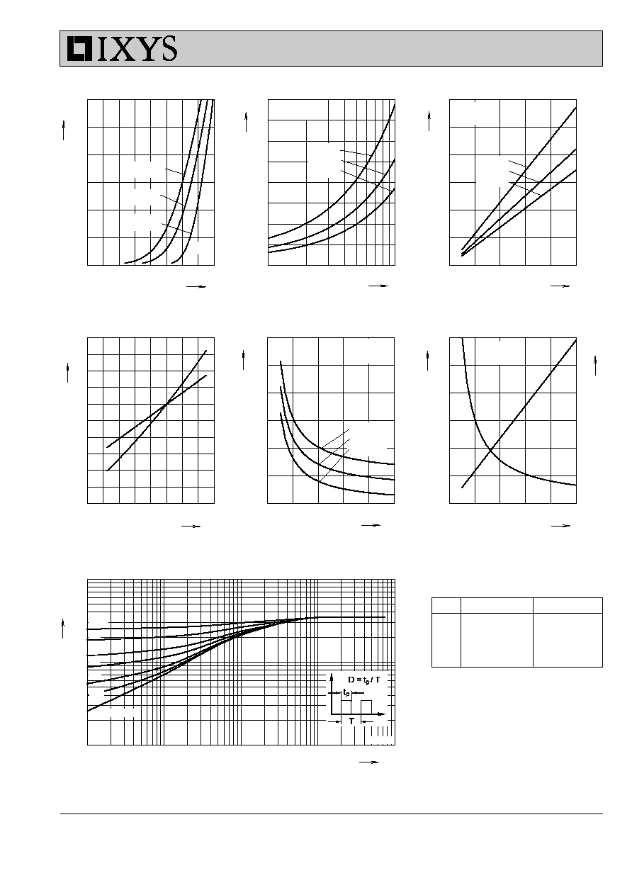
Fig. 3 Peak reverse current I
RM
versus -di
F
/dt
Fig. 2 Reverse recovery charge Q
r
versus -di
F
/dt
Fig. 1 Forward current I
F
versus V
F
T
VJ
=100∞C
T
VJ
=150∞C
T
VJ
= 100∞C
V
R
= 600V
T
VJ
= 100∞C
V
R
= 600V
I
F
=140A
I
F
= 70A
I
F
= 35A
Q
r
I
RM
Fig. 4 Dynamic parameters Q
r
, I
RM
versus T
VJ
Fig. 5 Recovery time t
rr
versus -di
F
/dt
Fig. 6 Peak forward voltage V
FR
and t
fr
versus di
F
/dt
I
F
=140A
I
F
= 70A
I
F
= 35A
t
fr
V
FR
Fig. 7 Transient thermal resistance junction to case
Constants for Z
thJC
calculation:
i
R
thi
(K/W)
t
i
(s)
1
0.017
0.00038
2
0.0184
0.0026
3
0.1296
0.0387
4
0.185
0.274
T
VJ
= 25∞C