1 - 4
© 2000 IXYS All rights reserved
Symbol
Test Conditions
Maximum Ratings
V
DSS
T
J
= 25
∞
C to 150
∞
C
N07
70
V
N06
60
V
V
DGR
T
J
= 25
∞
C to 150
∞
C; R
GS
= 1 M
W
N07
70
V
N06
60
V
V
GS
Continuous
±
20
V
V
GSM
Transient
±
30
V
I
D25
T
C
= 25
∞
C; Chip capability
200N06/200N07
200
A
180N07
180
A
I
L(RMS)
Terminal current limit
100
A
I
DM
T
C
= 25
∞
C, pulse width limited by T
JM
600
A
I
AR
T
C
= 25
∞
C
100
A
E
AR
T
C
= 25
∞
C
30
mJ
E
AS
T
C
= 25
∞
C
2
J
dv/dt
I
S
£
I
DM
, di/dt
£
100 A/
m
s, V
DD
£
V
DSS
,
5
V/ns
T
J
£
150
∞
C, R
G
= 2
W
P
D
T
C
= 25
∞
C
520
W
T
J
-55 ... +150
∞
C
T
JM
150
∞
C
T
stg
-55 ... +150
∞
C
V
ISOL
50/60 Hz, RMS
t = 1 min
2500
V~
I
ISOL
£
1 mA
t = 1 s
3000
V~
M
d
Mounting torque
1.5/13Nm/lb.in.
Terminal connection torque
1.5/13Nm/lb.in.
Weight
30
g
Symbol
Test Conditions
Characteristic Values
(T
J
= 25
∞
C, unless otherwise specified)
min.
typ.
max.
V
DSS
V
GS
= 0 V, I
D
= 1 mA
N06
60
V
N07
70
V
V
GS (th)
V
DS
= V
GS
, I
D
= 8 mA
2
4
V
I
GSS
V
GS
=
±
20 V
DC
, V
DS
= 0
±
200
nA
I
DSS
V
DS
= 0.8 ∑ V
DSS
T
J
= 25
∞
C
400
m
A
V
GS
= 0 V
T
J
= 125
∞
C
2
mA
R
DS(on)
V
GS
= 10 V, I
D
= 0.5 ∑ I
D25
200N06/200N07
6 m
W
Pulse test, t
£
300
m
s, duty cycle d
£
2 %
180N07
7 m
W
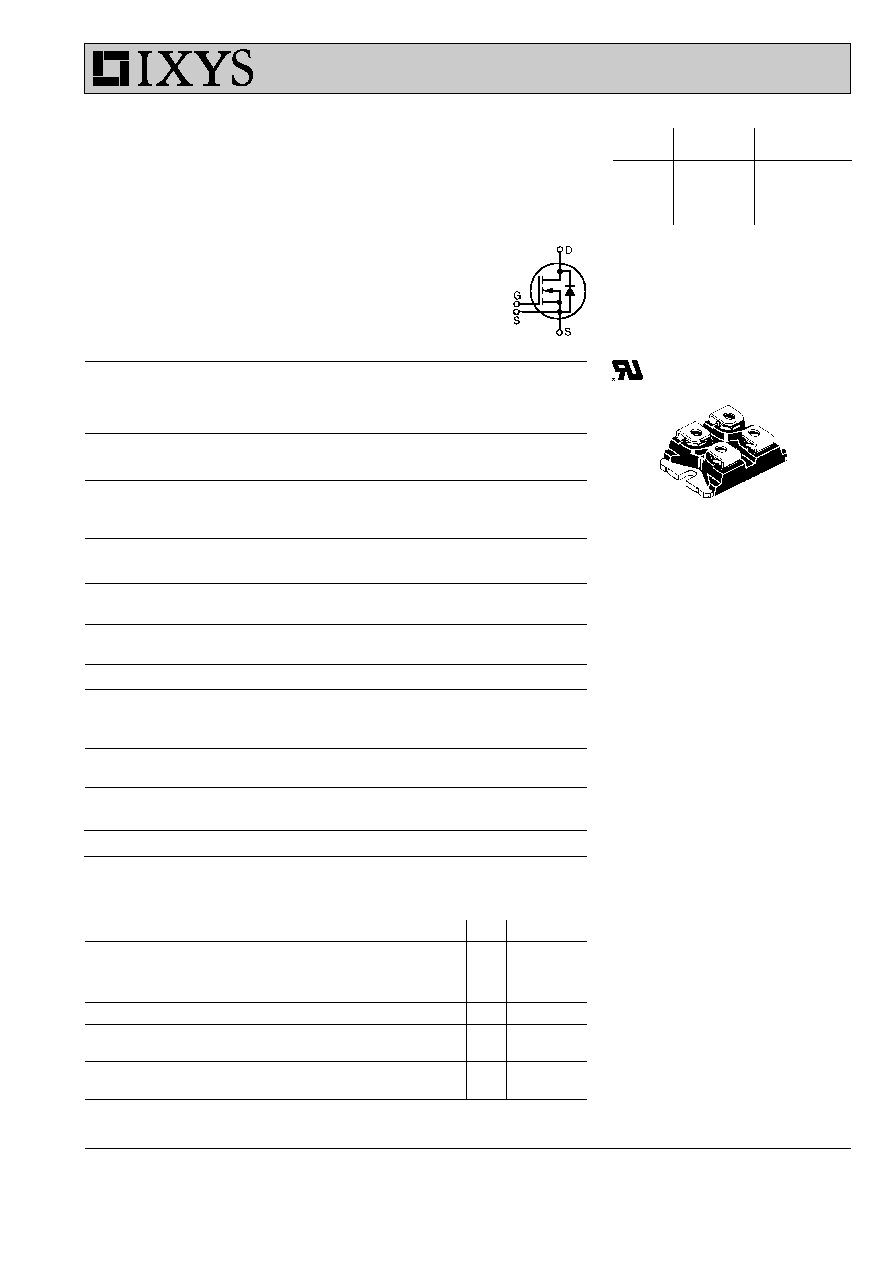
G = Gate
D = Drain
S = Source
Either Source terminal at miniBLOC can be used
as Main or Kelvin Source
Features
∑ International standard packages
∑ miniBLOC with Aluminium nitride
isolation
∑ Low R
DS (on)
HDMOS
TM
process
∑ Rugged polysilicon gate cell structure
∑ Unclamped Inductive Switching (UIS)
rated
∑ Low package inductance
∑ Fast intrinsic Rectifier
Applications
∑ DC-DC converters
∑ Synchronous rectification
∑ Battery chargers
∑ Switched-mode and resonant-mode
power supplies
∑ DC choppers
∑ Temperature and lighting controls
∑ Low voltage relays
Advantages
∑ Easy to mount
∑ Space savings
∑ High power density
S
G
S
D
miniBLOC, SOT-227 B (IXFN)
E153432
97533A (9/99)
HiPerFET
TM
Power MOSFETs
N-Channel Enhancement Mode
Avalanche Rated, High dv/dt, Low t
rr
V
DSS
I
D25
R
DS(on)
IXFN 200 N06
60 V
200 A
6 m
W
IXFN 180 N07
70 V
180 A
7 m
W
IXFN 200 N07
70 V
200 A
6 m
W
t
rr
£
250 ns
IXYS reserves the right to change limits, test conditions, and dimensions.
2 - 4
© 2000 IXYS All rights reserved
Symbol
Test Conditions
Characteristic Values
(T
J
= 25
∞
C, unless otherwise specified)
min.
typ.
max.
g
fs
V
DS
= 10 V; I
D
= 0.5 ∑ I
D25
, pulse test
60
80
S
C
iss
9000
pF
C
oss
V
GS
= 0 V, V
DS
= 25 V, f = 1 MHz
4000
pF
C
rss
2400
pF
t
d(on)
30
ns
t
r
V
GS
= 10 V, V
DS
= 0.5 ∑ V
DSS
, I
D
= 0.5 ∑ I
D25
60
ns
t
d(off)
R
G
= 1
W
(External),
100
ns
t
f
60
ns
Q
g(on)
480
nC
Q
gs
V
GS
= 10 V, V
DS
= 0.5 ∑ V
DSS
, I
D
= 0.5 ∑ I
D25
60
nC
Q
gd
240
nC
R
thJC
miniBLOC, SOT-227 B
0.24
K/W
R
thCK
miniBLOC, SOT-227 B
0.05
K/W
Source-Drain Diode
Characteristic Values
(T
J
= 25
∞
C, unless otherwise specified)
Symbol
Test Conditions
min.
typ.
max.
I
S
V
GS
= 0 V
200N06/200N07
200
A
180N07
180
A
I
SM
Repetitive; pulse width limited by T
JM
600
A
V
SD
I
F
= 100 A, V
GS
= 0 V,
1.7
V
Pulse test, t
£
300
m
s, duty cycle d
£
2 %
t
rr
150
250
ns
Q
RM
0.7
m
C
I
RM
9
A
I
F
= 25 A
-di/dt = 100 A/
m
s,
V
R
= 50 V
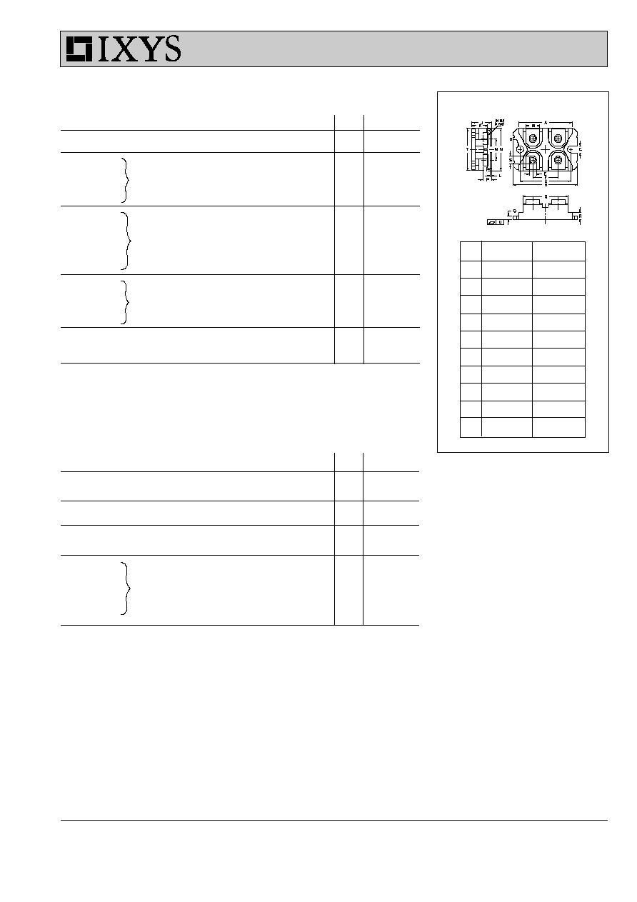
M4 screws (4x) supplied
Dim.
Millimeter
Inches
Min.
Max.
Min.
Max.
A
31.50
31.88
1.240
1.255
B
7.80
8.20
0.307
0.323
C
4.09
4.29
0.161
0.169
D
4.09
4.29
0.161
0.169
E
4.09
4.29
0.161
0.169
F
14.91
15.11
0.587
0.595
G
30.12
30.30
1.186
1.193
H
38.00
38.23
1.496
1.505
J
11.68
12.22
0.460
0.481
K
8.92
9.60
0.351
0.378
L
0.76
0.84
0.030
0.033
M
12.60
12.85
0.496
0.506
N
25.15
25.42
0.990
1.001
O
1.98
2.13
0.078
0.084
P
4.95
5.97
0.195
0.235
Q
26.54
26.90
1.045
1.059
R
3.94
4.42
0.155
0.174
S
4.72
4.85
0.186
0.191
T
24.59
25.07
0.968
0.987
U
-0.05
0.1
-0.002
0.004
miniBLOC, SOT-227 B
IXFN 200N06 IXFN 180N07 IXFN 200N07
IXYS MOSFETS and IGBTs are covered by one or more of the following U.S. patents:
4,835,592
4,881,106
5,017,508
5,049,961
5,187,117
5,486,715
4,850,072
4,931,844
5,034,796
5,063,307
5,237,481
5,381,025
3 - 4
© 2000 IXYS All rights reserved
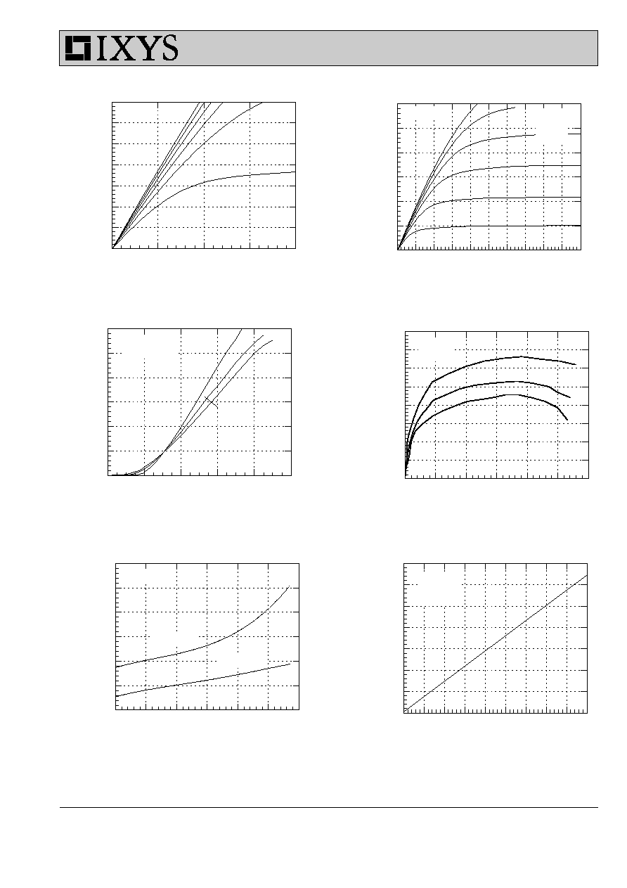
T
J
- Degrees C
-50 -25
0
25
50
75 100 125 150 175
R
DS
(O
N)
- Nor
m
alized
0.50
0.75
1.00
1.25
1.50
1.75
2.00
2.25
I
C
- Amperes
0
100
200
300
400
500
600
T
r
ans
c
onduc
tance
- Siem
ens
0
10
20
30
40
50
60
70
80
T
J
= 25
o
C
I
D
- Amperes
0
100
200
300
400
500
600
R
DS
(
O
N)
-
N
o
r
m
aliz
e
d
0.8
0.9
1.0
1.1
1.2
1.3
1.4
V
GS
- Volts
2
4
6
8
10
12
I
D
- A
m
per
e
s
0
100
200
300
400
500
600
V
DS
- Volts
0
1
2
3
4
5
6
7
8
9
10
I
D
- A
m
per
e
s
0
100
200
300
400
500
600
6V
7V
V
GS
= 15V
V
GS
= 10V
T
J
=25
O
C
V
GS
=10V
I
D
= 75A
V
GS
= 10V
V
DS
> 4R
DS(ON)
5V
T
J
=25
O
C
V
DS
- Volts
0.0
0.5
1.0
1.5
2.0
I
D
- A
m
per
e
s
0
25
50
75
100
125
150
175
T
J
= 25
o
C
V
GS
=10V
9V
8V
7V
6V
5V
T
J
= 25
O
C
V
GS
=10V
9V
8V
T
J
=150
O
C
T
J
=100
O
C
T
J
= 100
o
C
T
J
= 150
o
C
IXFN 200N06 IXFN 180N07 IXFN 200N07
Figure 1. Output Characteristics at 25
O
C
Figure 2. Extended Output Characteristics
Figure 6. Normalized R
DS(on)
vs. Junction
Temperature
Figure 3. Admittance Curves
Figure 5. R
DS(on)
normalized to 0.5 I
D25
value
Figure 4. Transconductance vs.
Drain Current
4 - 4
© 2000 IXYS All rights reserved
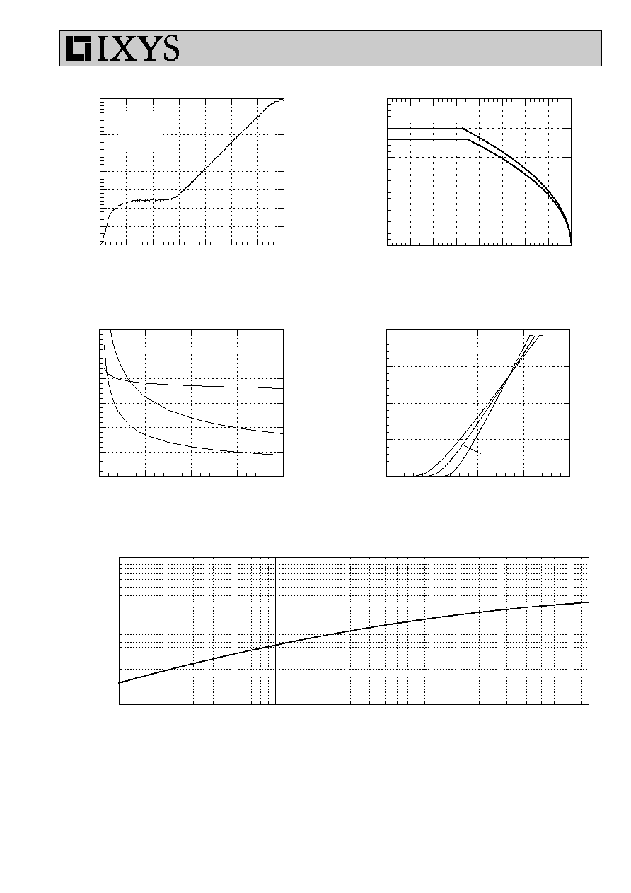
Time - Seconds
10
-3
10
-2
10
-1
10
0
Ther
m
al R
esponse -
K
/
W
10
-2
10
-1
10
0
V
DS
- Volts
0
10
20
30
40
pp
0
2000
4000
6000
8000
10000
12000
Crss
Coss
Ciss
V
SD
- Volts
0.0
0.5
1.0
1.5
2.0
I
D
- A
m
per
e
s
0
100
200
300
400
T
J
=25
O
C
T
J
=150
O
C
Gate Charge - nCoulombs
0
100
200
300
400
500
600
700
V
GS
- Volts
0
2
4
6
8
10
12
14
16
Case Temperature -
O
C
-50
-25
0
25
50
75
100 125 150
I
D
- A
m
p
e
res
0
50
100
150
200
250
V
DS
= 40V
I
D
= 38A
I
G
= 1mA
T
J
=100
O
C
F = 1MHz
T
J
=150
O
C
IXFN200
IXFN180
IXFN 200N06 IXFN 180N07 IXFN 200N07
Figure 11. Transient Thermal Resistance
Figure 10. Source-Drain Voltage vs. Source Current
Figure 7. Gate Charge
Figure 9. Capacitance Curves
Figure 8. Drain Current vs. Case
Temperature
(Terminal current limit)