© 1999 IXYS All rights reserved
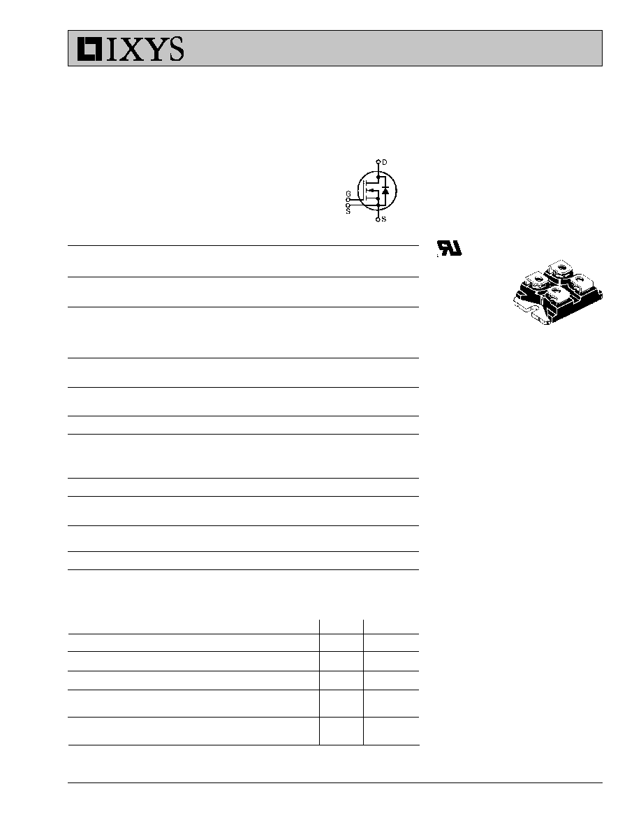
S
G
S
D
miniBLOC, SOT-227 B (IXFN)
E153432
Features
∑
International standard package
∑
Encapsulating
epoxy
meets
UL
94
V-0, flammability classification
∑
miniBLOC
with Aluminium nitride
isolation
∑
Low R
DS (on)
HDMOS
TM
process
∑
Rugged polysilicon gate cell structure
∑
Unclamped Inductive Switching (UIS)
rated
∑
Low package inductance
∑
Fast intrinsic Rectifier
Applications
∑
DC-DC converters
∑
Synchronous rectification
∑
Battery chargers
∑
Switched-mode and resonant-mode
power supplies
∑
DC choppers
∑
Temperature and lighting controls
∑
Low voltage relays
Advantages
∑
Easy to mount
∑
Space savings
∑
High power density
G = Gate
D = Drain
S = Source
Either Source terminal at miniBLOC can be used
as Main or Kelvin Source
Symbol
Test Conditions
Characteristic Values
(T
J
= 25
∞
C, unless otherwise specified)
Min. Typ. Max.
V
DSS
V
GS
= 0 V, I
D
= 3mA
100
V
V
GS(th)
V
DS
= V
GS
, I
D
= 8mA
2
4
V
I
GSS
V
GS
=
±
20V, V
GS
= 0V
±
100
nA
I
DSS
V
DS
= V
DSS
T
J
= 25
∞
C
100
µ
A
V
GS
= 0 V
T
J
= 125
∞
C
2
mA
R
DS(on)
V
GS
= 10V, I
D
= 0.5 ∑ I
D25
8
m
Note 2
98546B (8/99)
HiPerFET
TM
Power MOSFET
Single MOSFET Die
Symbol Test Conditions
Maximum Ratings
V
DSS
T
J
= 25∞C to 150∞C
100
V
V
DGR
T
J
= 25∞C to 150∞C, R
GS
= 1M
100
V
V
GS
Continuous
±
20
V
V
GSM
Transient
±
30
V
I
D25
T
C
= 25
∞
C
180
A
I
L(RMS)
Terminal (current limit)
100
A
I
DM
T
C
= 25
∞
C; Note 1
720 A
I
AR
T
C
= 25
∞
C
180 A
E
AR
T
C
= 25
∞
C
60
mJ
E
AS
T
C
= 25
∞
C
3
J
dv/dt
I
S
I
DM
, di/dt
100 A/
µ
s, V
DD
V
DSS
5 V/ns
T
J
150
∞
C, R
G
= 2
P
D
T
C
= 25
∞
C
600
W
T
J
-55 ... +150
∞
C
T
JM
150
∞
C
T
stg
-55 ... +150
∞
C
T
L
1.6 mm (0.063 in) from case for 10 s
300
∞
C
V
ISOL
50/60 Hz, RMS
t = 1 min
2500
V~
I
ISOL
1 mA
t = 1 s
3000
V~
M
d
Mounting torque
1.5/13 Nm/lb.in.
Terminal connection torque
1.5/13 Nm/lb.in.
Weight
30
g
IXFN 180N10
V
DSS
= 100 V
I
D25
= 180 A
R
DS(on)
= 8 m
t
rr
250 ns
Preliminary data sheet
IXYS MOSFETS and IGBTs are covered by one or more of the following U.S. patents: 4,835,592
4,881,106
5,017,508
5,049,961
5,187,117
5,486,715
4,850,072
4,931,844
5,034,796
5,063,307
5,237,481
5,381,025
IXYS reserves the right to change limits, test conditions, and dimensions.
Symbol
Test Conditions
Characteristic Values
(T
J
= 25
∞
C, unless otherwise specified)
Min.
Typ.
Max.
g
fs
V
DS
= 10 V; I
D
= 60A, Note 2
60
90
S
C
iss
9100
pF
C
oss
V
GS
= 0 V, V
DS
= 25 V, f = 1 MHz
3200
pF
C
rss
1600
pF
t
d(on)
50
ns
t
r
V
GS
= 10 V, V
DS
= 0.5 ∑ V
DSS
, I
D
= 0.5 ∑ I
D25
90
ns
t
d(off)
R
G
= 1
(External),
140
ns
t
f
65
ns
Q
g(on)
360
nC
Q
gs
V
GS
= 10 V, V
DS
= 0.5 ∑ V
DSS
, I
D
= 0.5 ∑ I
D25
65
nC
Q
gd
190
nC
R
thJC
LOC, SOT-227 B
0.21
K/W
R
thCK
miniBLOC, SOT-227 B
0.05
K/W
Source-Drain Diode
(T
J
= 25
∞
C, unless otherwise specified)
Characteristic Values
Symbol
Test Conditions
Min.
Typ. Max.
I
S
V
GS
= 0
180
A
I
SM
Repetitive;
720
A
pulse width limited by T
JM
V
SD
I
F
= 100 A, V
GS
= 0 V,
1.5
V
Pulse test, t
300
µ
s, duty cycle d
2 %
t
rr
250
n s
Q
RM
I
F
= 50 A, -di/dt = 100 A/
µ
s, V
R
= 50 V
1.1
µ
C
I
RM
1 3
A
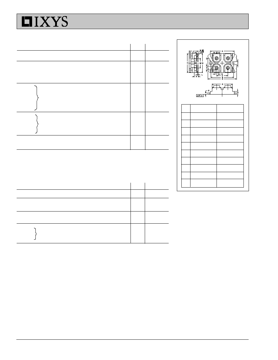
M4 screws (4x) supplied
Dim.
Millimeter
Inches
Min.
Max.
Min.
Max.
A
31.50
31.88
1.240
1.255
B
7.80
8.20
0.307
0.323
C
4.09
4.29
0.161
0.169
D
4.09
4.29
0.161
0.169
E
4.09
4.29
0.161
0.169
F
14.91
15.11
0.587
0.595
G30.12
30.30
1.186
1.193
H
38.00
38.23
1.496
1.505
J
11.68
12.22
0.460
0.481
K
8.92
9.60
0.351
0.378
L
0.76
0.84
0.030
0.033
M
12.60
12.85
0.496
0.506
N
25.15
25.42
0.990
1.001
O
1.98
2.13
0.078
0.084
P
4.95
5.97
0.195
0.235
Q
26.54
26.90
1.045
1.059
R
3.94
4.42
0.155
0.174
S
4.72
4.85
0.186
0.191
T
24.59
25.07
0.968
0.987
U
-0.05
0.1
-0.002
0.004
miniBLOC, SOT-227 B
Notes:
1.
Pulse width limited by T
JM.
2.
Pulse test, t
300 ms, duty cycle d
2 %
IXFN 180N10
© 1999 IXYS All rights reserved
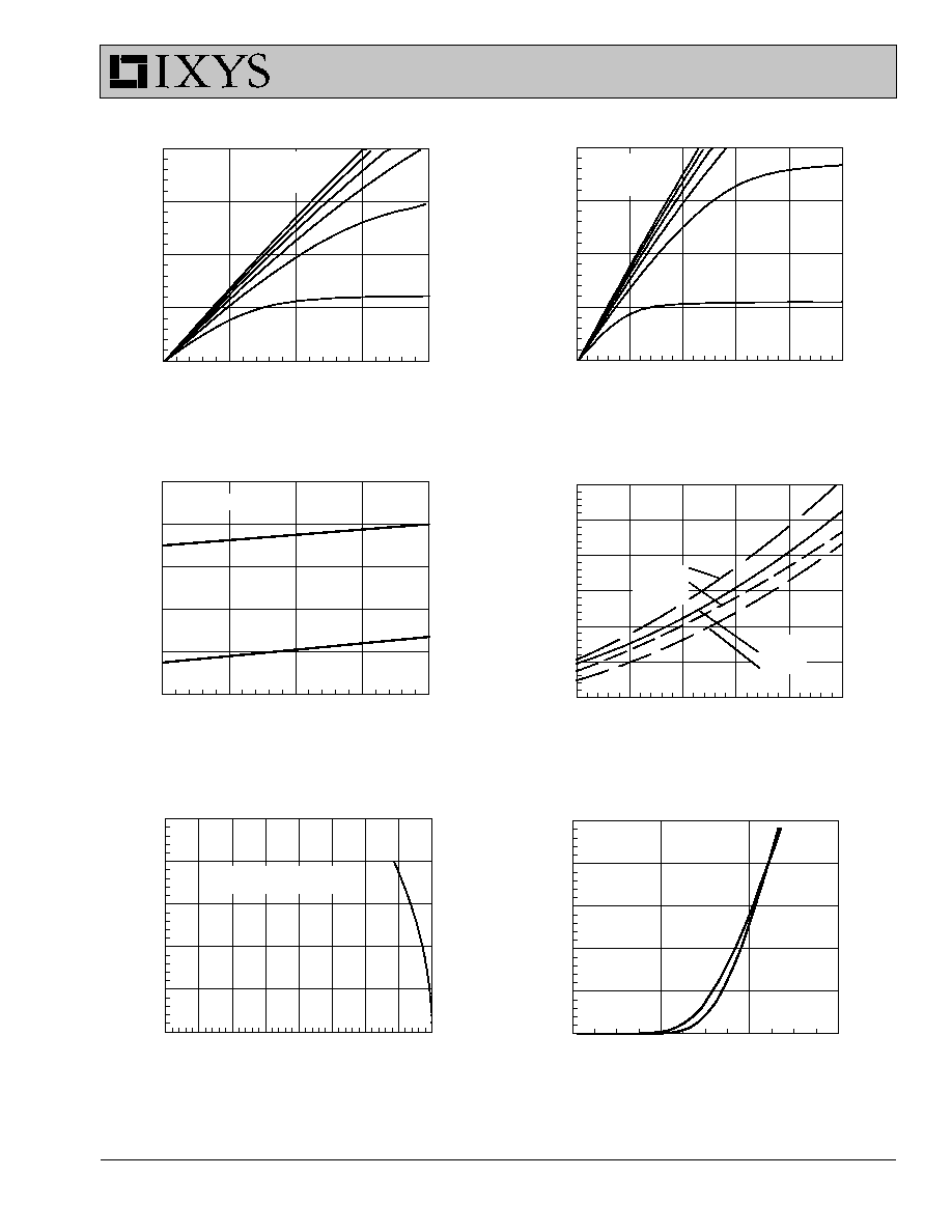
T
C
- Degrees C
-50 -25
0
25
50
75 100 125 150
I
D
- A
m
p
e
r
e
s
0
25
50
75
100
125
V
DS
- Volts
0
1
2
3
4
5
I
D
- A
m
p
e
r
e
s
0
50
100
150
200
V
GS
- Volts
2
4
6
8
I
D
- A
m
per
e
s
0
20
40
60
80
100
T
J
- Degrees C
25
50
75
100
125
150
R
DS
(O
N)
- Nor
m
a
l
i
z
ed
0.8
1.0
1.2
1.4
1.6
1.8
2.0
I
D
- Amperes
0
50
100
150
200
R
DS
(O
N)
-
Nor
m
a
liz
ed
0.8
1.0
1.2
1.4
1.6
1.8
V
DS
- Volts
0.0
0.5
1.0
1.5
2.0
I
D
- A
m
per
e
s
0
50
100
150
200
5V
V
GS
= 10V
V
GS
=10V
9V
8V
T
J
=125
O
C
T
J
=25
O
C
6V
6V
5V
T
J
= 25
o
C
I
D
=180A
T
J
= 25
O
C
T
J
= 125
o
C
V
GS
=10V
9V
8V
T
J
= 125
O
C
7V
7V
V
GS
=10V
V
GS
=15V
V
GS
=10V
V
GS
=15V
I
D
=90A
Terminal Current Limit
IXFN 180N10
Figure 3. R
DS(on)
normalized to 15A/25
O
C vs. I
D
Figure 5. Drain Current vs. Case Temperature
Figure 6. Admittance Curves
Figure 1. Output Characteristics at 25
O
C
Figure 2. Output Characteristics at 125
O
C
Figure 4. R
DS(on)
normalized to 15A/25
O
C vs. T
J
IXYS reserves the right to change limits, test conditions, and dimensions.
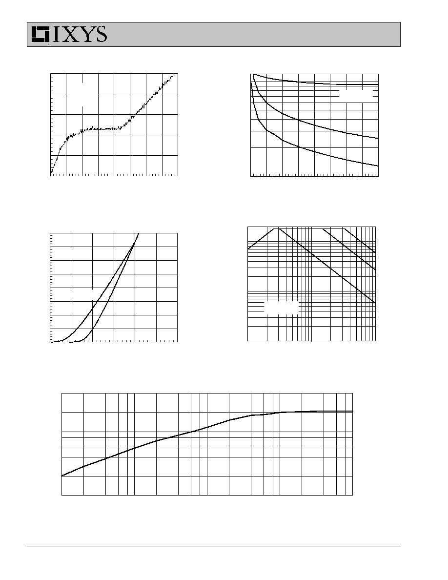
Pulse Width - Seconds
10
-3
10
-2
10
-1
10
0
10
1
R
(th
)
JC
- K/W
0.02
0.04
0.06
0.08
0.20
0.40
0.01
0.10
V
DS
- Volts
0
5
10
15
20
25
30
35
40
C
a
pa
ci
ta
nc
e -
pF
1000
10000
V
SD
- Volts
0.4
0.6
0.8
1.0
1.2
1.4
1.6
I
D
- A
m
p
e
r
e
s
0
25
50
75
100
125
150
175
200
Gate Charge - nC
0
50
100 150 200 250 300 350 400
V
GS
- V
o
l
t
s
0
3
6
9
12
15
Crss
Coss
Ciss
T
J
=25
O
C
V
DS
=50V
I
D
=90A
I
G
=10mA
F = 100kHz
V
DS
- Volts
1
10
100
I
D
- A
m
pe
r
e
s
1
10
100
T
C
= 25
O
C
10 ms
1 ms
DC
200
V
GS
= 0V
T
J
=125
O
C
IXFN 180N10
Figure 7. Gate Charge
Figure 8. Capacitance Curves
Figure 9. Forward Voltage Drop of the Intrinsic Diode
Figure 10. Forward Bias Safe Operating Area
Figure 11. Transient Thermal Resistance