© 2005 IXYS All rights reserved
IXFA 12N50P
IXFP 12N50P
Symbol
Test Conditions
Maximum Ratings
V
DSS
T
J
= 25
∞C to 150∞C
500
V
V
DGR
T
J
= 25
∞C to 150∞C; R
GS
= 1 M
500
V
V
GSM
Transient
± 40
V
V
GSM
Continuous
± 30
V
I
D25
T
C
= 25
∞C
12
A
I
DM
T
C
= 25
∞C, pulse width limited by T
JM
20
A
I
AR
T
C
= 25
∞C
12
A
E
AR
T
C
= 25
∞C
24
mJ
E
AS
T
C
= 25
∞C
600
mJ
dv/dt
I
S
I
DM
, di/dt
100 A/s, V
DD
V
DSS
,
20
V/ns
T
J
150∞C, R
G
= 10
P
D
T
C
= 25
∞C
200
W
T
J
-55 ... +150
∞C
T
JM
150
∞C
T
stg
-55 ... +150
∞C
T
L
1.6 mm (0.062 in.) from case for 10 s
300
∞C
Plastic body for 10 seconds
260
∞C
M
d
Mounting torque
(TO-220)
1.13/10 Nm/lb.in.
Weight
TO-220
4
g
TO-263
3
g
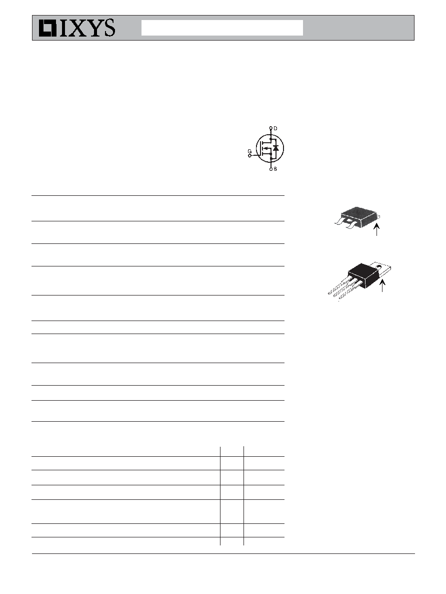
G = Gate
D = Drain
S = Source
TAB = Drain
Symbol
Test Conditions
Characteristic Values
(T
J
= 25
∞C unless otherwise specified)
Min. Typ.
Max.
V
DSS
V
GS
= 0 V, I
D
= 250
A
500
V
V
GS(th)
V
DS
= V
GS
, I
D
= 1 mA
3.0
5.5
V
I
GSS
V
GS
=
± 30 V
DC
, V
DS
= 0
±100
nA
I
DSS
V
DS
= V
DSS
5
A
V
GS
= 0 V
T
J
= 125
∞C
150
A
R
DS(on)
V
GS
= 10 V, I
D
= 0.5 I
D25
, Note 1
500 m
PolarHV
TM
Power
MOSFET
N-Channel Enhancement Mode
Avalanche Rated
IXFA 12N50P
IXFP 12N50P
V
DSS
= 500
V
I
D25
=
12
A
R
DS(on)
0.5
t
rr
200
ns
DS99436(09/05)
Advance Technical Information
TO-220 (IXFP)
D
(TAB)
G
S
TO-263 (IXFA)
G
S
(TAB)
Features
International standard packages
Unclamped Inductive Switching (UIS)
rated
Low package inductance
- easy to drive and to protect
Advantages
Easy to mount
Space savings
High power density
IXYS reserves the right to change limits, test conditions, and dimensions.
IXFA 12N50P
IXFP 12N50P
IXYS MOSFETs and IGBTs are covered by 4,835,592
4,931,844
5,049,961
5,237,481
6,162,665
6,404,065 B1
6,683,344
6,727,585
one or more of the following U.S. patents:
4,850,072
5,017,508
5,063,307
5,381,025
6,259,123 B1
6,534,343
6,710,405B2
6,759,692
4,881,106
5,034,796
5,187,117
5,486,715
6,306,728 B1
6,583,505
6,710,463
6771478 B2
Symbol
Test Conditions Characteristic Values
(T
J
= 25
∞C unless otherwise specified)
Min.
Typ.
Max.
g
fs
V
DS
= 20 V; I
D
= 0.5 I
D25
, Note 1
13
S
C
iss
1690
pF
C
oss
V
GS
= 0 V, V
DS
= 25 V, f = 1 MHz
182
pF
C
rss
16
pF
t
d(on)
22
ns
t
r
V
GS
= 10 V, V
DS
= 0.5 V
DSS
, I
D
= I
D25
27
ns
t
d(off)
R
G
= 50
(External)
65
ns
t
f
20
ns
Q
g(on)
29
nC
Q
gs
V
GS
= 10 V, V
DS
= 0.5 V
DSS
, I
D
= 0.5 I
D25
11
nC
Q
gd
10
nC
R
thJC
0.62 K/W
R
thCK
(TO-220)
0.25
KW
Source-Drain Diode Characteristic Values
T
J
= 25
∞C unless otherwise specified)
Symbol
Test Conditions
Min.
Typ.
Max.
I
S
V
GS
= 0 V
44
A
I
SM
Repetitive
132
A
V
SD
I
F
= I
S
, V
GS
= 0 V, Note 1
1.5
V
t
rr
I
F
= 22 A, -di/dt = 100 A/
s
200
ns
Q
RM
V
R
= 100 V, V
GS
= 0 V
0.4
C
I
RM
4f
A
Note 1:
Pulse test, t
300 s, duty cycle d 2 %
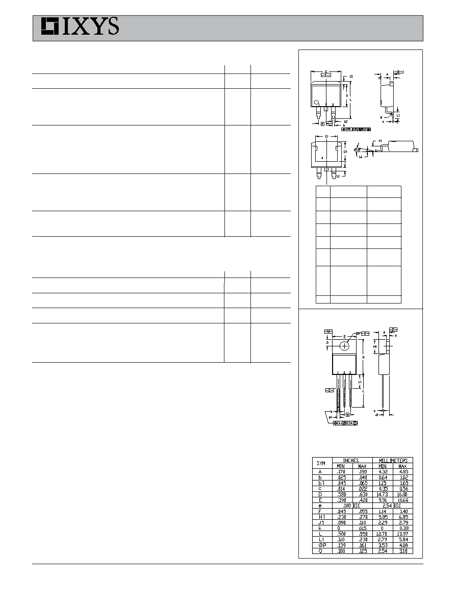
Pins:
1 - Gate
2 - Drain
3 - Source
4 - Drain
TO-220 (IXTP) Outline
Dim.
Millimeter
Inches
Min.
Max.
Min.
Max.
A
4.06
4.83
.160
.190
A1
2.03
2.79
.080
.110
b
0.51
0.99
.020
.039
b2
1.14
1.40
.045
.055
c
0.46
0.74
.018
.029
c2
1.14
1.40
.045
.055
D
8.64
9.65
.340
.380
D1
7.11
8.13
.280
.320
E
9.65
10.29
.380
.405
E1
6.86
8.13
.270
.320
e
2.54
BSC
.100
BSC
L
14.61
15.88
.575
.625
L1
2.29
2.79
.090
.110
L2
1.02
1.40
.040
.055
L3
1.27
1.78
.050
.070
L4
0
0.38
0
.015
R
0.46
0.74
.018
.029
TO-263 (IXTA) Outline
Pins:
1 - Gate 2, 4 - Drain
3 - Source
© 2005 IXYS All rights reserved
IXFA 12N50P
IXFP 12N50P
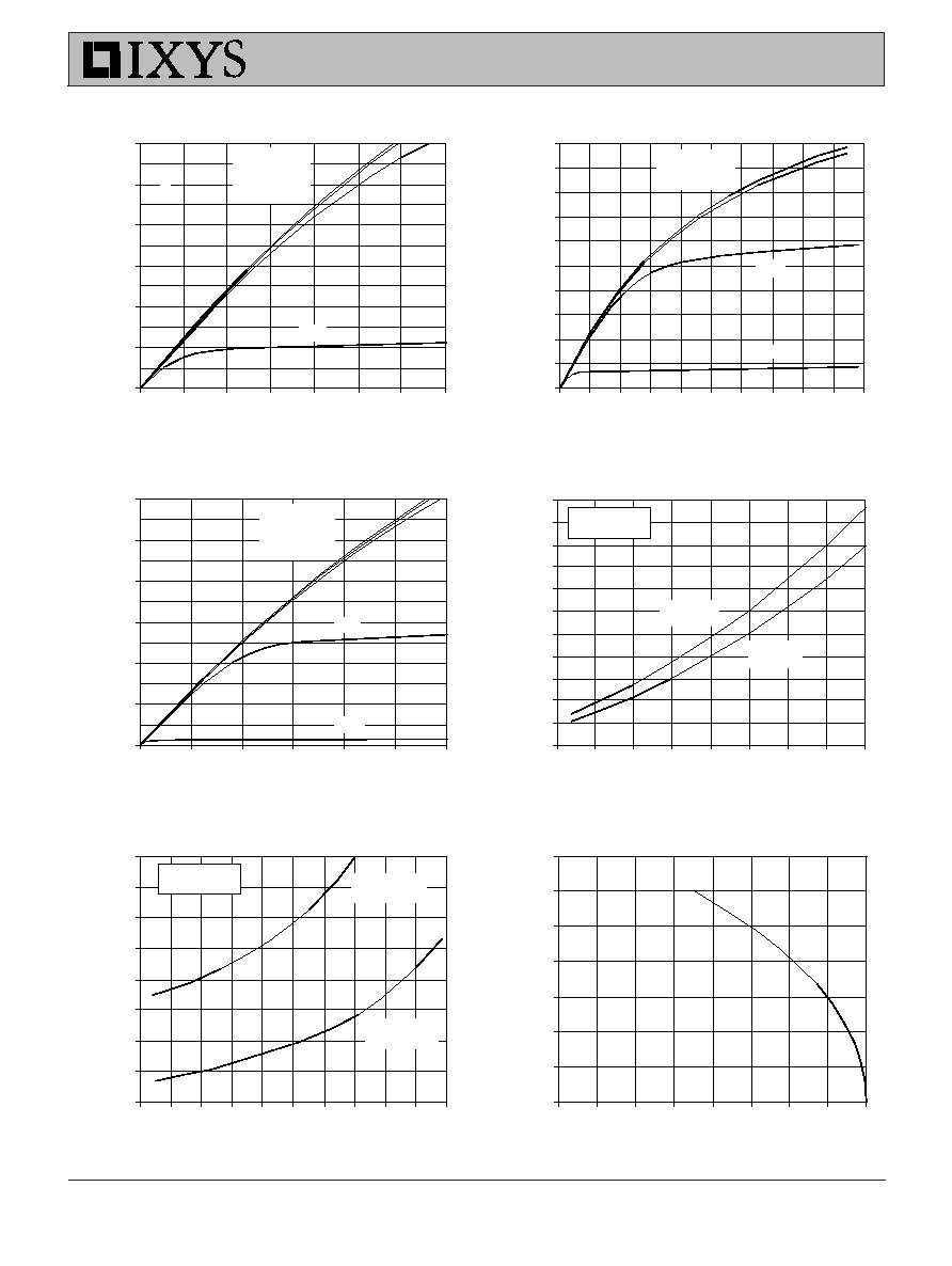
Fig. 2. Extended Output Characteristics
@ 25
∫
C
0
3
6
9
12
15
18
21
24
27
30
0
3
6
9
12
15
18
21
24
27
30
V
D S
- Volts
I
D
-
A
m
p
e
re
s
V
GS
= 10V
8V
7V
6V
Fig. 3. Output Characteristics
@ 125
∫
C
0
2
4
6
8
10
12
0
2
4
6
8
10
12
V
D S
- Volts
I
D
-
A
m
per
es
V
GS
= 10V
8V
7V
5V
6V
Fig. 1. Output Characteristics
@ 25
∫
C
0
2
4
6
8
10
12
0
1
2
3
4
5
6
7
V
D S
- Volts
I
D
-
A
m
per
es
V
GS
= 10V
8V
7V
6V
Fig. 4. R
DS(on
)
Norm alized to 0.5 I
D25
Value vs. Junction Tem perature
0.4
0.6
0.8
1
1.2
1.4
1.6
1.8
2
2.2
2.4
2.6
-50
-25
0
25
50
75
100
125
150
T
J
- Degrees Centigrade
R
D
S
(
o n )
-
N
o
rm
a
l
i
z
e
d
I
D
= 12A
I
D
= 6A
V
GS
= 10V
Fig. 6. Drain Current vs. Case
Tem perature
0
2
4
6
8
10
12
14
-50
-25
0
25
50
75
100
125
150
T
C
- Degrees Centigrade
I
D
-
A
m
per
es
Fig. 5. R
DS(on)
Norm alized to
0.5 I
D25
Value vs. I
D
0.7
1
1.3
1.6
1.9
2.2
2.5
2.8
3.1
0
3
6
9
12
15
18
21
24
27
30
I
D
- Amperes
R
D
S
(
o n )
-
N
o
rm
a
l
i
z
e
d
T
J
= 125
∫
C
T
J
= 25
∫
C
V
GS
= 10V
IXYS reserves the right to change limits, test conditions, and dimensions.
IXFA 12N50P
IXFP 12N50P
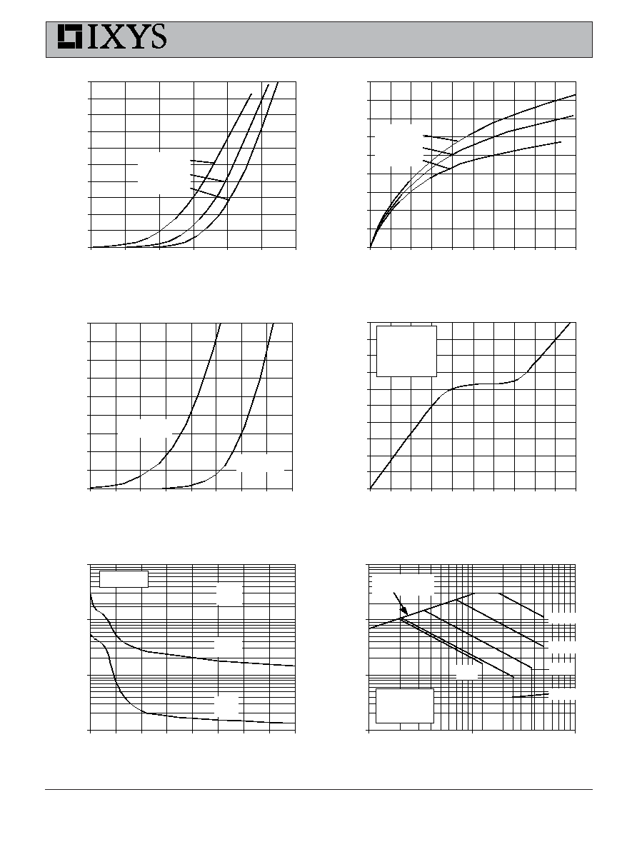
Fig. 11. Capacitance
10
100
1000
10000
0
5
10
15
20
25
30
35
40
V
D S
- Volts
C
a
pac
i
t
anc
e -
pi
c
o
F
a
r
a
d
s
Ciss
Coss
Crs
f = 1MHz
Fig. 10. Gate Charge
0
1
2
3
4
5
6
7
8
9
10
0
3
6
9
12
15
18
21
24
27
30
Q
G
- nanoCoulombs
V
G S
- V
o
l
t
s
V
DS
= 250V
I
D
= 6A
I
G
= 10mA
Fig. 7. Input Adm ittance
0
2
4
6
8
10
12
14
16
18
20
4.5
5
5.5
6
6.5
7
7.5
V
G S
- Volts
I
D
- A
m
p
e
re
s
T
J
= 125
∫
C
25
∫
C
-40
∫
C
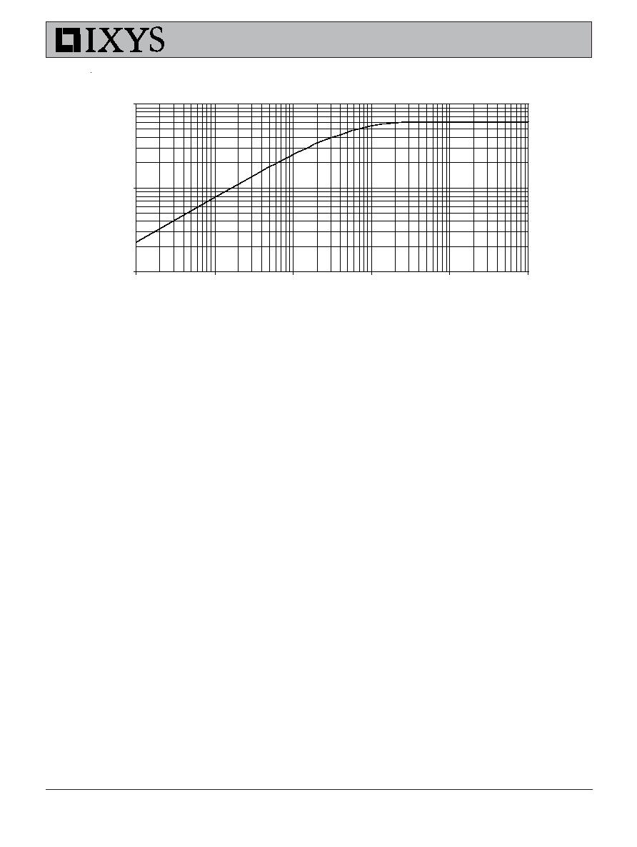
Fig. 8. Transconductance
0
3
6
9
12
15
18
21
24
27
0
2
4
6
8
10
12
14
16
18
20
I
D
- Amperes
g
f s
- S
i
e
m
e
n
s
T
J
= -40
∫
C
25
∫
C
125
∫
C
Fig. 9. Source Current vs.
Source-To-Drain Voltage
0
1
2
3
4
5
6
7
8
9
0.45
0.5
0.55
0.6
0.65
0.7
0.75
0.8
0.85
V
S D
- Volts
I
S
-
A
m
p
e
re
s
T
J
= 125
∫
C
T
J
= 25
∫
C
Fig. 12. Forw ard-Bias
Safe Operating Area
0.1
1
10
100
10
100
1000
V
D S
- Volts
I
D
- A
m
p
e
re
s
100s
1ms
DC
T
J
= 150∫C
T
C
= 25∫C
R
DS(on)
Limit
10ms
25s
© 2005 IXYS All rights reserved
IXFA 12N50P
IXFP 12N50P
Fig. 13. Maxim um Transient Therm al Resistance
0.01
0.10
1.00
0.01
0.1
1
10
100
1000
Pulse Width - milliseconds
R
( t h ) J
C
-
∫
C /
W