
© 2004 IXYS All rights reserved
DS99312(10/05)
PolarHV
TM
HiPerFET
Power MOSFET
(Electrically Isolated Back Surface)
V
DSS
= 500
V
I
D25
=
18
A
R
DS(on)
190 m
t
rr
250
ns
N-Channel Enhancement Mode
Avalanche Rated
Fast Intrinsic Diode
Features
International standard isolated
packages
UL recognized packages
Silicon chip on Direct-Copper-Bond
substrate
- High power dissipation
- Isolated mounting surface
- 2500V electrical isolation
Unclamped Inductive Switching (UIS)
rated
Low package inductance
- easy to drive and to protect
Fast intrinsic diode
Advantages
Easy to mount
Space savings
High power density
Symbol
Test Conditions
Characteristic Values
(T
J
= 25
∞C unless otherwise specified)
Min. Typ.
Max.
V
DSS
V
GS
= 0 V, I
D
= 250
A
500
V
V
GS(th)
V
DS
= V
GS
, I
D
= 4 mA
2.5
5.0
V
I
GSS
V
GS
=
± 30 V
DC
, V
DS
= 0
± 100
nA
I
DSS
V
DS
= V
DSS
25
A
V
GS
= 0 V
T
J
= 125
∞C
250
A
R
DS(on)
V
GS
= 10 V, I
D
= I
T
190
m
Symbol
Test Conditions
Maximum Ratings
V
DSS
T
J
= 25
∞C to 150∞C
500
V
V
DGR
T
J
= 25
∞C to 150∞C; R
GS
= 1 M
500
V
V
GSS
Continuous
± 30
V
V
GSM
Transient
± 40
V
I
D25
T
C
= 25
∞C
18
A
I
DM
T
C
= 25
∞C, pulse width limited by T
JM
100
A
I
AR
T
C
= 25
∞C
24
A
E
AR
T
C
= 25
∞C
50
mJ
E
AS
T
C
= 25
∞C
1.5
J
dv/dt
I
S
I
DM
, di/dt
100 A/s, V
DD
V
DSS
,
20
V/ns
T
J
150∞C, R
G
= 4
P
D
T
C
= 25
∞C
156
W
T
J
-55 ... +150
∞C
T
JM
150
∞C
T
stg
-55 ... +150
∞C
T
L
1.6 mm (0.062 in.) from case for 10 s
300
∞C
V
ISOL
50/60 Hz, RMS, 1 minute
2500
V~
F
C
Mounting Force
(IXFC)
11..65 / 2.5..15
N/lb
(IXFR)
20..120 / 4.5..25N/lb
Weight
(IXFC)
3
g
(IXFR)
5
g
G = Gate
D = Drain
S = Source
Advance Technical Information
IXFC 36N50P
IXFR 36N50P
G
D
S
ISOPLUS247 (IXFR)
E153432
G
D
S
ISOPLUS220 (IXFC)
E153432
Isolated back
surface*
Isolated back
surface
IXYS reserves the right to change limits, test conditions, and dimensions.
IXFC 36N50P
IXFR 36N50P
Symbol
Test Conditions
Characteristic Values
(T
J
= 25
∞C, unless otherwise specified)
Min.
Typ. Max.
g
fs
V
DS
= 20 V; I
D
=
T
, Note 1
25
35
S
C
iss
4800
pF
C
oss
V
GS
= 0 V, V
DS
= 25 V, f = 1 MHz
510
pF
C
rss
60
pF
t
d(on)
29
ns
t
r
V
GS
= 10 V, V
DS
= 0.5 I
D25
23
ns
t
d(off)
R
G
= 4
(External)
82
ns
t
f
23
ns
Q
g(on)
135
nC
Q
gs
V
GS
= 10 V, V
DS
= 0.5 V
DSS
, I
D
= I
T
30
nC
Q
gd
65
nC
R
thJC
0.8
K/W
R
thCK
0.15
K/W
Source-Drain Diode
Characteristic Values
(T
J
= 25
∞C, unless otherwise specified)
Symbol
Test Conditions
min.
typ.
max.
I
S
V
GS
= 0 V
24
A
I
SM
Repetitive
100
A
V
SD
I
F
= I
S
, V
GS
= 0 V,
1.5
V
t
rr
I
F
= 25A, -di/dt = 100 A/
s
250
ns
Q
RM
V
R
= 100 V; V
GS
= 0 V
0.6
C
IXYS MOSFETs and IGBTs are covered by
4,835,592
4,931,844
5,049,961
5,237,481
6,162,665
6,404,065 B1
6,683,344
6,727,585
one or moreof the following U.S. patents:
4,850,072
5,017,508
5,063,307
5,381,025
6,259,123 B1
6,534,343
6,710,405B2
6,759,692
4,881,106
5,034,796
5,187,117
5,486,715
6,306,728 B1
6,583,505
6,710,463
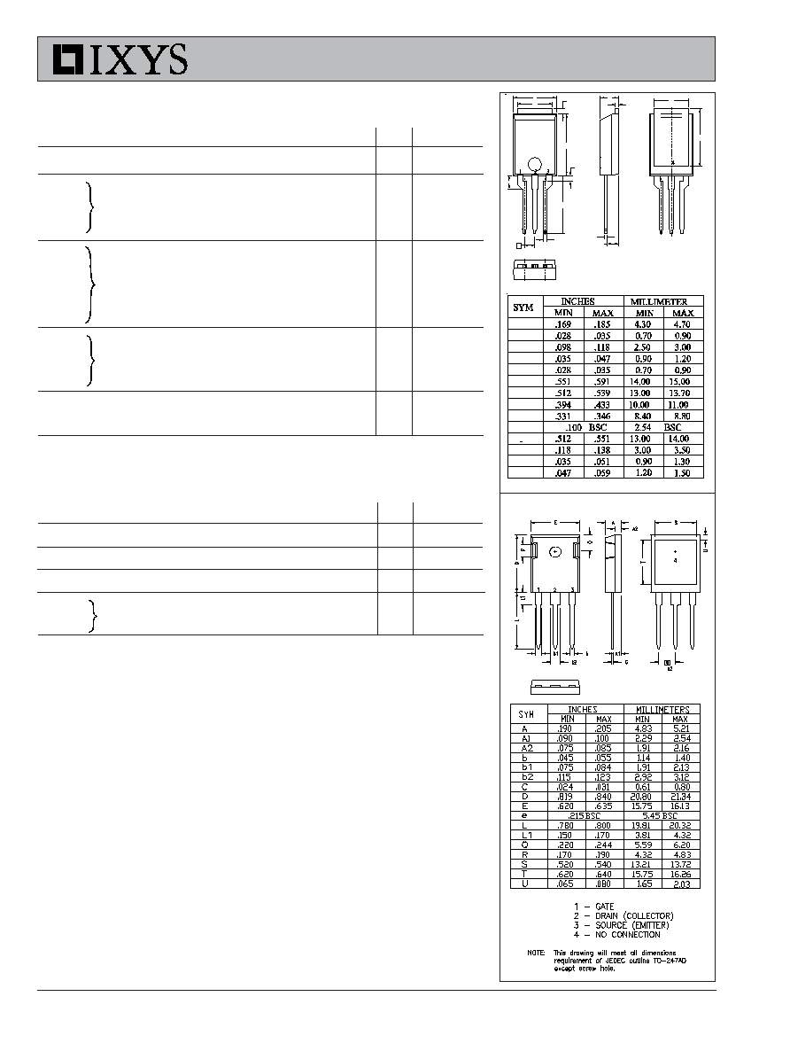
ISOPLUS247 Outline
Notes:
1.
Pulse test, t
300 s, duty cycle d 2 %;
2. Test current I
T
= 18A.
D1
L
L3
L1
E1
e
E
b
D
c
A2
A1
A
L2
Terminals: 1-Gate 2-Drain
E1
E
L2
D
L3
L
L1
3X b
2X e
c
A2
A1
A
E1
D1
© 2004 IXYS All rights reserved
IXFC 36N50P
IXFR 36N50P
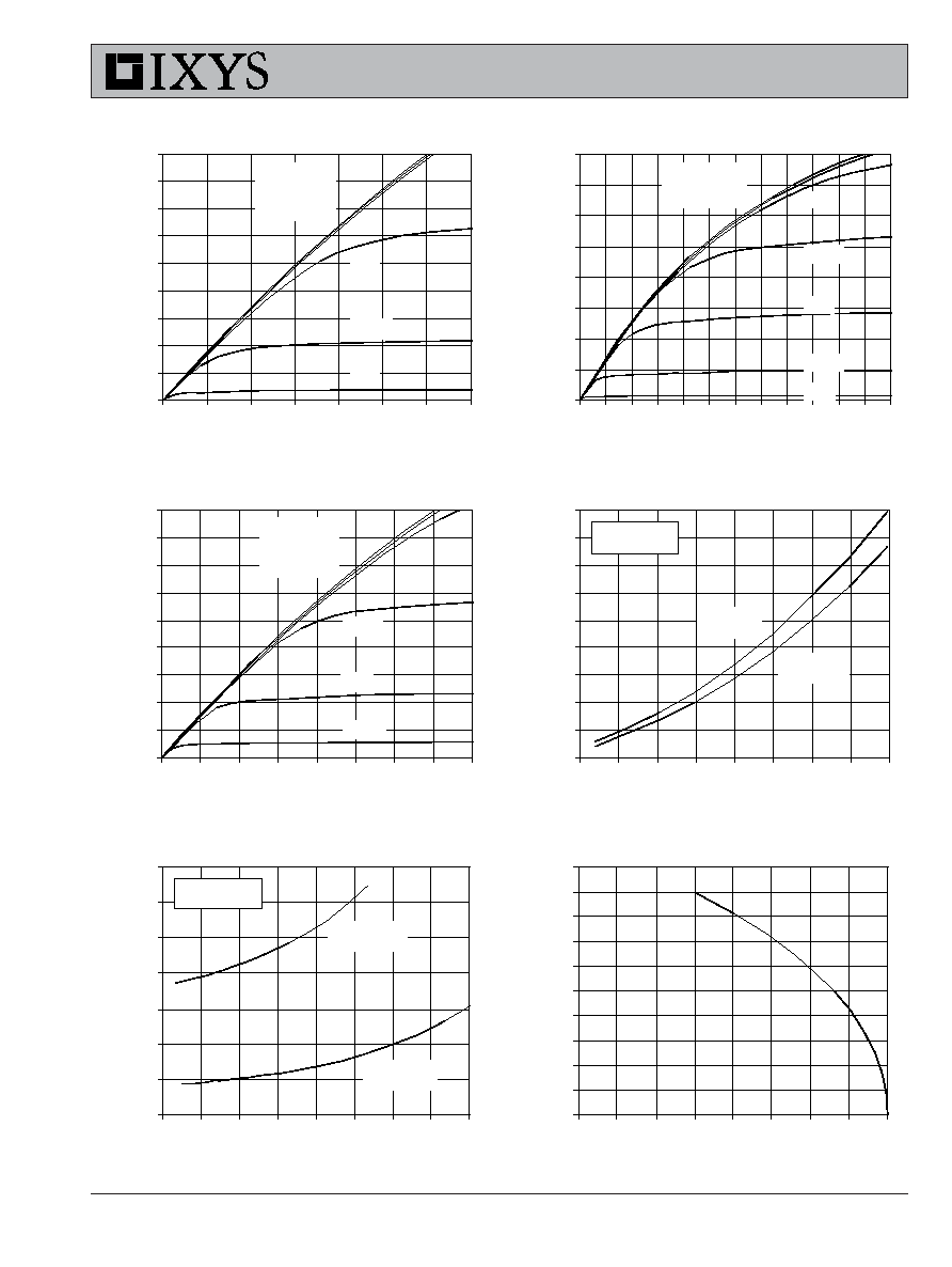
Fig. 2. Extended Output Characteristics
@ 25
∫
C
0
10
20
30
40
50
60
70
80
0
2
4
6
8
10
12
14
16
18
20
22
24
V
D S
- Volts
I
D
-
A
m
per
es
V
GS
= 10V
8V
5.5V
5V
6V
6.5V
7V
Fig. 3. Output Characteristics
@ 125
∫
C
0
4
8
12
16
20
24
28
32
36
0
2
4
6
8
10
12
14
16
V
D S
- Volts
I
D
-
A
m
per
es
V
GS
= 10V
7V
6V
4.5V
5V
5.5V
Fig. 1. Output Characteristics
@ 25
∫
C
0
4
8
12
16
20
24
28
32
36
0
1
2
3
4
5
6
7
V
D S
- Volts
I
D
- A
m
p
e
re
s
V
GS
= 10V
8V
7V
5V
6V
5.5V
Fig. 4. R
DS(on
)
Norm alized to I
D25
Value
vs. Junction Tem perature
0.4
0.7
1
1.3
1.6
1.9
2.2
2.5
2.8
3.1
-50
-25
0
25
50
75
100
125
150
T
J
- Degrees Centigrade
R
D S
(
o
n
)
- N
o
rm
a
l
i
z
e
d
I
D
= 36A
I
D
= 18A
V
GS
= 10V
Fig. 5. R
DS(on)
Norm alized to
I
D25
Value vs. I
D
0.6
1
1.4
1.8
2.2
2.6
3
3.4
0
10
20
30
40
50
60
70
80
I
D
- Amperes
R
D
S
(
o n )
-
N
o
rm
a
l
i
z
e
d
T
J
= 125∫C
T
J
= 25∫C
V
GS
= 10V
Fig. 6. Drain Current vs. Case
Tem perature
0
2
4
6
8
10
12
14
16
18
20
-50
-25
0
25
50
75
100
125
150
T
C
- Degrees Centigrade
I
D
-
A
m
per
es
IXYS reserves the right to change limits, test conditions, and dimensions.
IXFC 36N50P
IXFR 36N50P
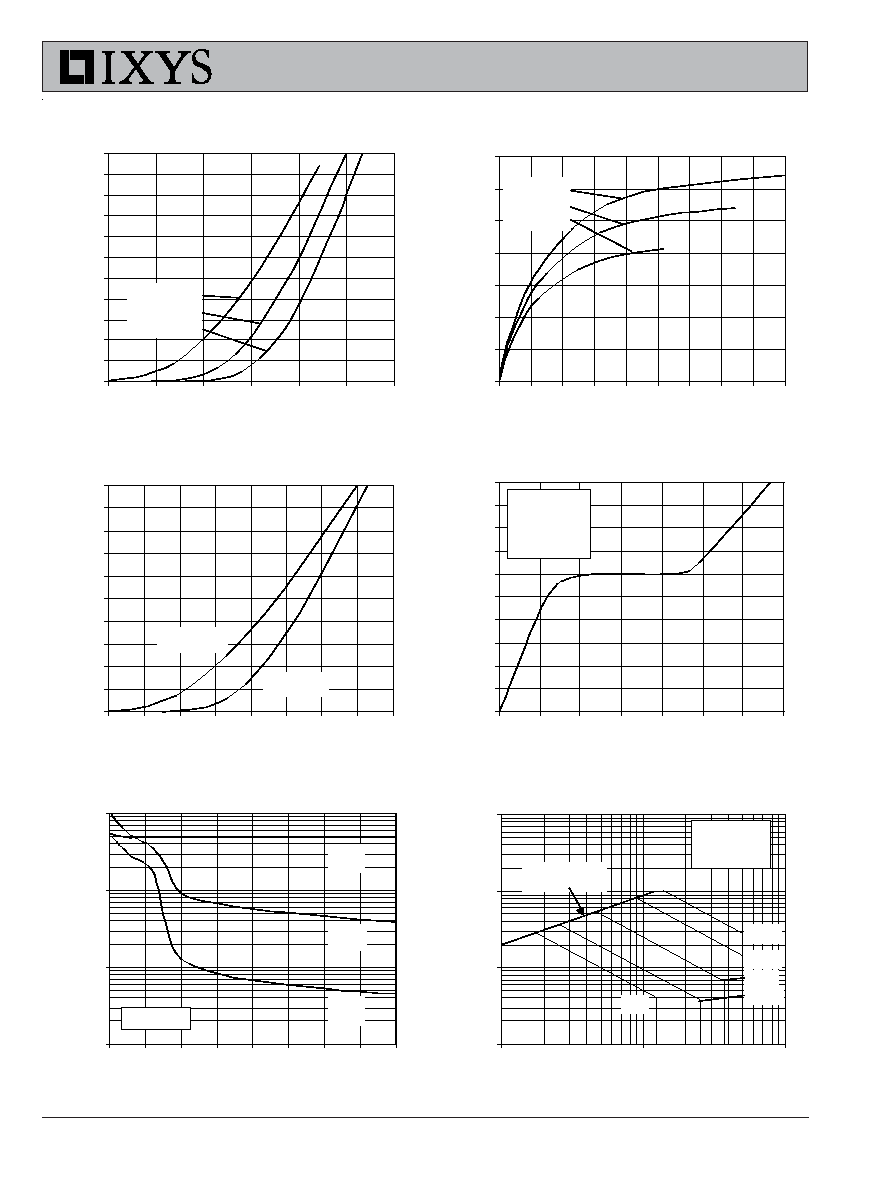
Fig. 11. Capacitance
10
100
1000
10000
0
5
10
15
20
25
30
35
40
V
D S
- Volts
C
apac
i
t
anc
e -
pi
c
o
F
a
r
ads
Ciss
Coss
Crss
f = 1MHz
Fig. 10. Gate Charge
0
1
2
3
4
5
6
7
8
9
10
0
20
40
60
80
100
120
140
Q
G
- nanoCoulombs
V
G S
-
V
o
l
t
s
V
DS
= 250V
I
D
= 18A
I
G
= 10mA
Fig. 7. Input Adm ittance
0
5
10
15
20
25
30
35
40
45
50
55
4
4.5
5
5.5
6
6.5
7
V
G S
- Volts
I
D
-
A
m
per
es
T
J
= 125∫C
25∫C
-40∫C
Fig. 8. Transconductance
0
10
20
30
40
50
60
70
0
10
20
30
40
50
60
70
80
90
I
D
- Amperes
g
f s
-
S
i
e
m
e
n
s
T
J
= -40∫C
25∫C
125∫C
Fig. 9. Source Current vs.
Source-To-Drain Voltage
0
10
20
30
40
50
60
70
80
90
100
0.4
0.5
0.6
0.7
0.8
0.9
1
1.1
1.2
V
S D
- Volts
I
S
- A
m
p
e
r
e
s
T
J
= 125∫C
T
J
= 25∫C
Fig. 12. Forw ard-Bias
Safe Operating Area
1
10
100
1000
10
100
1000
V
D S
- Volts
I
D
-
A
m
per
es
100s
1ms
DC
T
J
= 150∫C
T
C
= 25∫C
R
DS(on)
Limit
10ms
25s
© 2004 IXYS All rights reserved
IXFC 36N50P
IXFR 36N50P
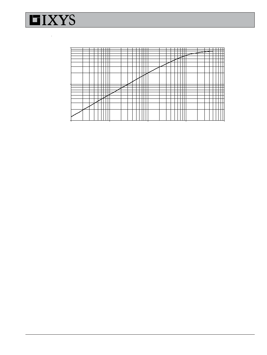
Fig. 13. Maxim um Transient Therm al Resistance
0.01
0.10
1.00
0.1
1
10
100
1000
Pulse Width - milliseconds
R
( t h ) J
C
-
∫
C /
W