© 2004 IXYS All rights reserved
Symbol
Test Conditions
Maximum Ratings
V
DSS
T
J
= 25
∞C to 150∞C
500
V
V
DGR
T
J
= 25
∞C to 150∞C; R
GS
= 1 M
500
V
V
GS
Continuous
±30
V
V
GSM
Transient
±40
V
I
D25
T
C
= 25
∞C
29
A
I
DM
T
C
= 25
∞C, pulse width limited by T
JM
160
A
I
AR
T
C
= 25
∞C
40
A
E
AR
T
C
= 25
∞C
50
mJ
E
AS
T
C
= 25
∞C
2.5
J
dv/dt
I
S
I
DM
, di/dt
100 A/µs, V
DD
V
DSS
,
20
V/ns
T
J
150∞C, R
G
= 2
P
D
T
C
= 25
∞C
320
W
T
J
-55 ... +150
∞C
T
JM
150
∞C
T
stg
-55 ... +150
∞C
T
L
1.6 mm (0.063 in) from case for 10 s
300
∞C
F
C
Mounting force
22...130/5...30
N/lb.
Weight
5
g
HiPerFET
TM
Power MOSFETs
N-Channel Enhancement Mode
Avalanche Rated, Low Q
g
Low R
g
, High dv/dt, Low t
rr
Features
Double metal process for low gate
resistance
International standard packages
Epoxy
meet
UL
94
V-0, flammability
classification
Low R
DS (on)
, low Q
g
Avalanche energy and current rated
Fast intrinsic rectifier
Applications
DC-DC converters
Switched-mode and resonant-mode
power supplies, >500kHz switching
DC choppers
Pulse generation
Laser drivers
Advantages
Easy to mount
Space savings
High power density
Symbol
Test Conditions
Characteristic Values
(T
J
= 25
∞C, unless otherwise specified)
min.
typ.
max.
V
DSS
V
GS
= 0 V, I
D
= 250
µA
500
V
V
GS(th)
V
DS
= V
GS
, I
D
= 4 mA
2.5
5.0
V
I
GSS
V
GS
=
±30 V
DC
, V
DS
= 0
±200 nA
I
DSS
V
DS
= V
DSS
T
J
= 25
∞C
25
µA
V
GS
= 0 V
T
J
= 125
∞C
1
mA
R
DS(on)
V
GS
= 10 V, I
D
= I
T
0.17
Pulse test, t
300 µs, duty cycle d 2 %
DS99075B(05/04)
IXFR40N50Q2
V
DSS
= 500 V
I
D25
= 29 A
R
DS(on)
= 0.17
t
rr
250 ns
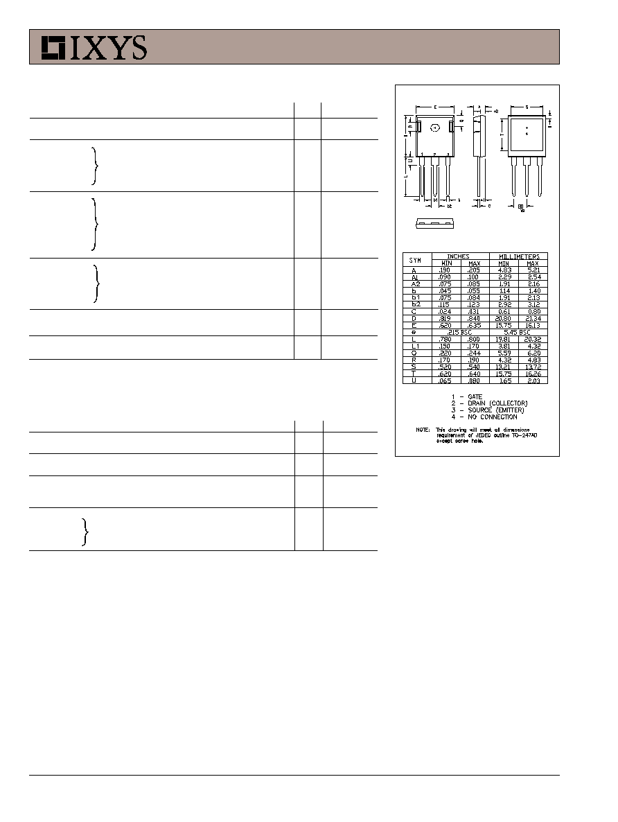
G = Gate
D = Drain
S = Source
TAB = Isolated
G
D
S
(TAB)
Preliminary Data Sheet
ISOPLUS247 (IXFR)
E153432
IXYS reserves the right to change limits, test conditions, and dimensions.
IXYS MOSFETs and IGBTs are covered by one or more
4,850,072
4,931,844
5,034,796
5,063,307
5,237,481
5,381,025
6,404,065B1 6,162,665
6,534,343
6,583,505
of the following U.S. patents:
4,835,592
4,881,106
5,017,508
5,049,961
5,187,117
5,486,715
6,306,728B1
6,259,123B1 6,306,728B1 6,683,344
Symbol
Test Conditions
Characteristic Values
(T
J
= 25
∞C, unless otherwise specified)
min.
typ.
max.
g
fs
V
DS
= 10 V; I
D
= I
T
, pulse test
15
28
S
C
iss
4200
pF
C
oss
V
GS
= 0 V, V
DS
= 25 V, f = 1 MHz
680
pF
C
rss
170
pF
t
d(on)
17
ns
t
r
V
GS
= 10 V, V
DS
= 0.5 ∑ V
DSS
, I
D
= I
T
13
ns
t
d(off)
R
G
= 2
(External),
42
ns
t
f
8
ns
Q
g(on)
110
nC
Q
gs
V
GS
= 10 V, V
DS
= 0.5 ∑ V
DSS
, I
D
= I
T
25
nC
Q
gd
50
nC
R
thJC
0.39
K/W
R
thCK
0.15
K/W
Source-Drain Diode
Characteristic Values
(T
J
= 25
∞C, unless otherwise specified)
Symbol
Test Conditions
min.
typ. max.
I
S
V
GS
= 0 V
40
A
I
SM
Repetitive; pulse width limited by T
JM
160
A
V
SD
I
F
= I
S
, V
GS
= 0 V,
1.5
V
Pulse test, t
300 µs, duty cycle d 2 %
t
rr
250
ns
Q
RM
1
µC
I
RM
9
A
I
F
= 25A -di/dt = 100 A/
µs, V
R
= 100 V
IXFR40N50Q2
TO-264 AA Outline
ISOPLUS247 Outline
Note: Test current I
T
= 20A
© 2004 IXYS All rights reserved
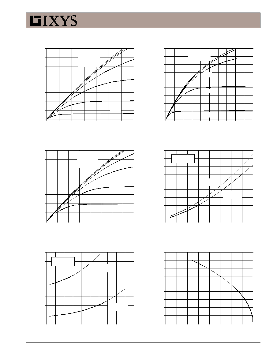
Fig. 2. Extended Output Characteristics
@ 25
∫
C
0
10
20
30
40
50
60
70
80
90
0
3
6
9
12
15
18
21
24
27
30
V
D S
- Volts
I
D
-
A
m
per
es
V
GS
= 10V
8V
7V
6V
5V
Fig. 3. Output Characteristics
@ 125
∫
C
0
5
10
15
20
25
30
35
40
0
2
4
6
8
10
12
14
16
V
D S
- Volts
I
D
-
A
m
per
es
V
GS
= 10V
8V
7V
4.5V
5.5V
5V
6V
Fig. 1. Output Characteristics
@ 25
∫
C
0
5
10
15
20
25
30
35
40
0
1
2
3
4
5
6
7
V
D S
- Volts
I
D
-
A
m
per
es
V
GS
= 10V
8V
7V
5V
4.5V
5.5V
6V
Fig. 4. R
DS(on
)
Norm alized to 0.5 I
D25
Value vs. Junction Tem perature
0.4
0.7
1
1.3
1.6
1.9
2.2
2.5
2.8
3.1
-50
-25
0
25
50
75
100
125
150
T
J
- Degrees Centigrade
R
D
S
(
o n )
-
N
o
rm
a
l
i
z
e
d
I
D
= 40A
I
D
= 20A
V
GS
= 10V
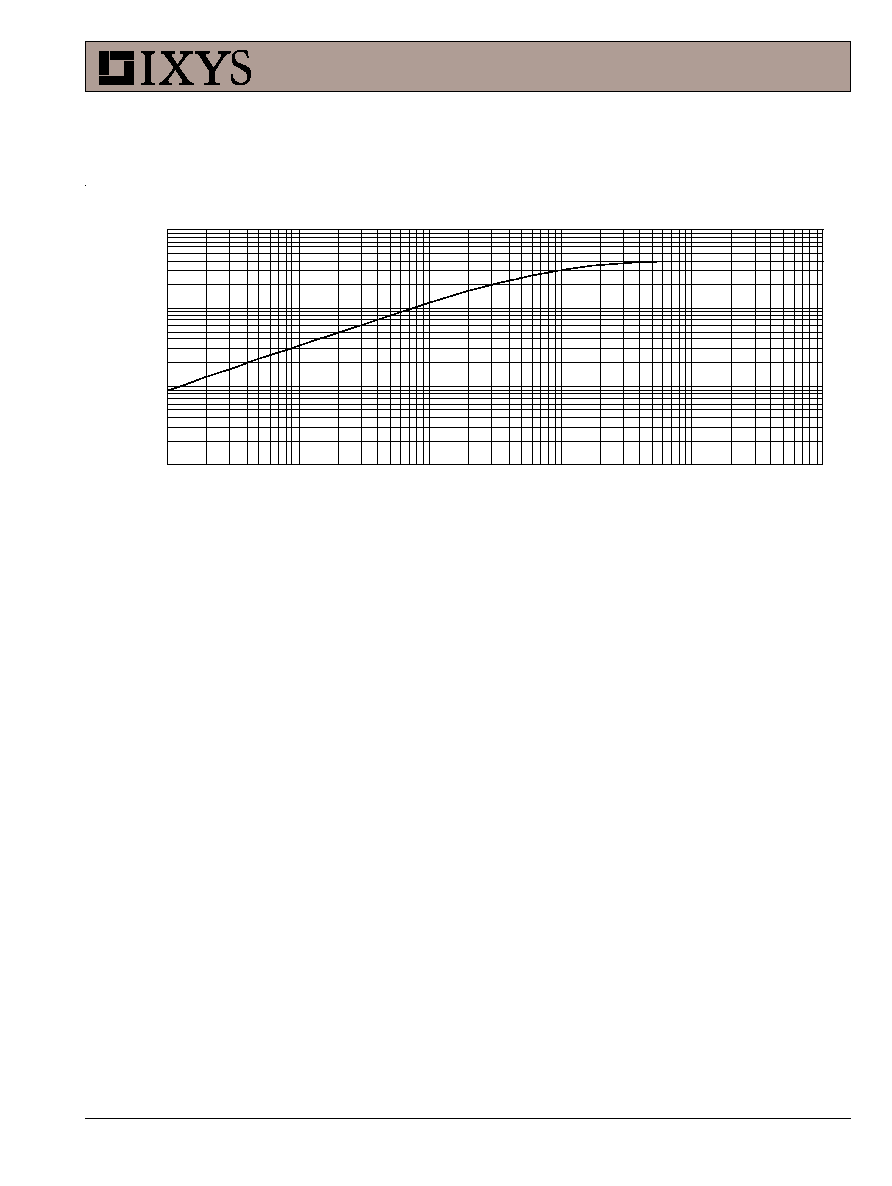
Fig. 6. Drain Current vs. Case
Tem perature
0
5
10
15
20
25
30
35
40
45
-50
-25
0
25
50
75
100
125
150
T
C
- Degrees Centigrade
I
D
-
A
m
per
e
s
Fig. 5. R
DS(on)
Norm alized to
0.5 I
D25
Value vs. I
D
0.7
1
1.3
1.6
1.9
2.2
2.5
2.8
3.1
0
10
20
30
40
50
60
70
80
90
100
I
D
- Amperes
R
D
S
(
o n )
- N
o
rm
a
l
i
z
e
d
T
J
= 125∫C
T
J
= 25∫C
V
GS
= 10V
IXFR40N50Q2
IXYS reserves the right to change limits, test conditions, and dimensions.
IXYS MOSFETs and IGBTs are covered by one or more
4,850,072
4,931,844
5,034,796
5,063,307
5,237,481
5,381,025
6,404,065B1 6,162,665
6,534,343
6,583,505
of the following U.S. patents:
4,835,592
4,881,106
5,017,508
5,049,961
5,187,117
5,486,715
6,306,728B1
6,259,123B1 6,306,728B1 6,683,344
IXFR40N50Q2
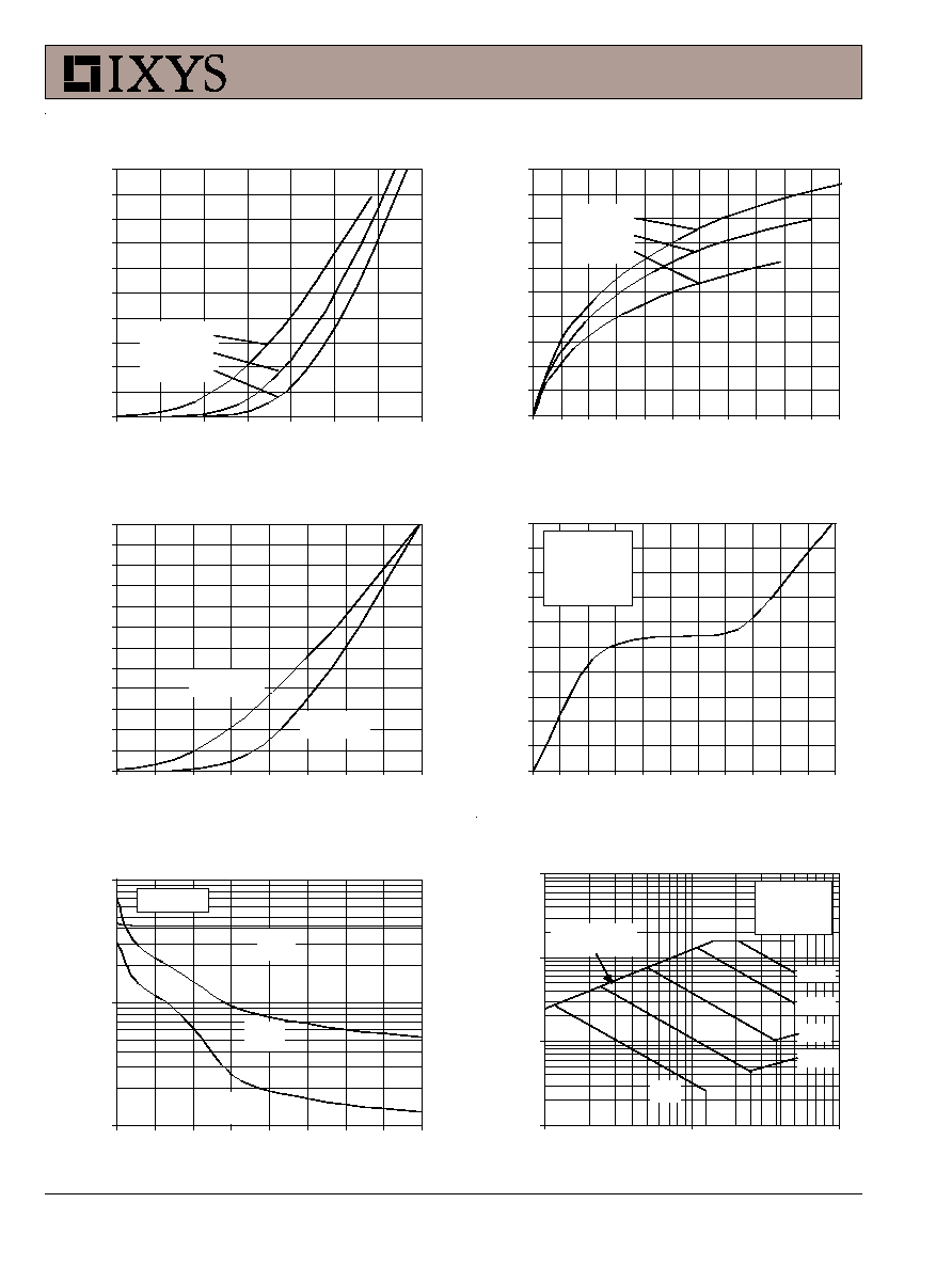
Fig. 11. Capacitance
100
1000
10000
0
5
10
15
20
25
30
35
40
V
D S
- Volts
C
apac
i
t
anc
e -
pi
c
o
F
a
r
ads
Ciss
Coss
Crss
f = 1MHz
Fig. 10. Gate Charge
0
1
2
3
4
5
6
7
8
9
10
0
10
20
30
40
50
60
70
80
90 100 110
Q
G
- nanoCoulombs
V
G S
-
V
o
l
t
s
V
DS
= 250V
I
D
= 20A
I
G
= 10mA
Fig. 7. Input Adm ittance
0
5
10
15
20
25
30
35
40
45
50
3
3.5
4
4.5
5
5.5
6
6.5
V
G S
- Volts
I
D
-
A
m
p
e
re
s
T
J
= 125∫C
25∫C
-40∫C
Fig. 8. Transconductance
0
5
10
15
20
25
30
35
40
45
50
0
5
10
15
20
25
30
35
40
45
50
55
I
D
- Amperes
g
f s
-
S
i
em
ens
T
J
= -40∫C
25∫C
125∫C
Fig. 9. Source Current vs.
Source-To-Drain Voltage
0
10
20
30
40
50
60
70
80
90
100
110
120
0.4
0.5
0.6
0.7
0.8
0.9
1
1.1
1.2
V
S D
- Volts
I
S
-
A
m
per
es
T
J
= 125∫C
T
J
= 25∫C
Fig. 12. Forw ard-Bias
Safe Ope rating Are a
1
10
100
1000
10
100
1000
V
D S
- Volts
I
D
- Am
peres
100µs
1ms
D C
T
J
= 150∫C
T
C
= 25∫C
R
DS(on)
Lim it
10m s
25µs
© 2004 IXYS All rights reserved
IXFR40N50Q2
Fig . 1 3 . M a x im u m T r a n s ie n t T h e r m a l Re s is t a n c e
0 . 0 0
0 . 0 1
0 . 1 0
1 . 0 0
0 . 1
1
1 0
1 0 0
1 0 0 0
1 0 0 0 0
Pu ls e W id th - millis e c o n d s
R
( t h ) J
C
-
∫
C /
W