© 2003 IXYS All rights reserved
Symbol
Test Conditions
Maximum Ratings
V
DSS
T
J
= 25
∞
C to 150
∞
C
200
V
V
DGR
T
J
= 25
∞
C to 150
∞
C; R
GS
= 1 M
200
V
V
GS
Continuous
±
20
V
V
GSM
Transient
±
30
V
I
D25
T
C
= 25
∞
C
50
A
I
DM
T
C
= 25
∞
C, Note 1
232
A
I
AR
T
C
= 25
∞
C
58
A
E
AR
T
C
= 25
∞
C
30
mJ
E
AS
T
C
= 25
∞
C
1.0
J
dv/dt
I
S
I
DM
, di/dt
100 A/
µ
s, V
DD
V
DSS
5
V/ns
T
J
150
∞
C, R
G
= 2
P
D
T
C
= 25
∞
C
300
W
T
J
-55 ... +150
∞
C
T
JM
150
∞
C
T
stg
-55 ... +150
∞
C
T
L
1.6 mm (0.062 in.) from case for 10 s
250
∞
C
V
ISOL
50/60 Hz, RMS
t = 1 min
2500
V~
Weight
5
g
Symbol
Test Conditions
Characteristic Values
(T
J
= 25
∞
C, unless otherwise specified)
min.
typ.
max.
V
DSS
V
GS
= 0 V, I
D
= 250
µ
A
200
V
V
GS(th)
V
DS
= V
GS
, I
D
= 4mA
2.0
4.0 V
I
GSS
V
GS
=
±
20 V, V
DS
= 0
±
100 nA
I
DSS
V
DS
= V
DSS
T
J
= 25
∞
C
25
µ
A
V
GS
= 0 V
T
J
= 125
∞
C
1 mA
R
DS(on)
V
GS
= 10 V, I
D
= 29A
40 m
Note 2
DS98591B(01/03)
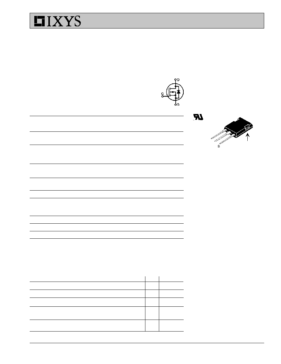
G
D
Features
Silicon chip on Direct-Copper-Bond
substrate
- High power dissipation
- Isolated mounting surface
- 2500V electrical isolation
Low drain to tab capacitance(<50pF)
IXYS advanced low Q
g
process
Rugged polysilicon gate cell structure
Unclamped Inductive Switching (UIS)
rated
Fast intrinsic diode
Applications
DC-DC converters
Battery chargers
Switched-mode and resonant-mode
power supplies
DC choppers
AC motor control
Advantages
Easy assembly
Space savings
High power density
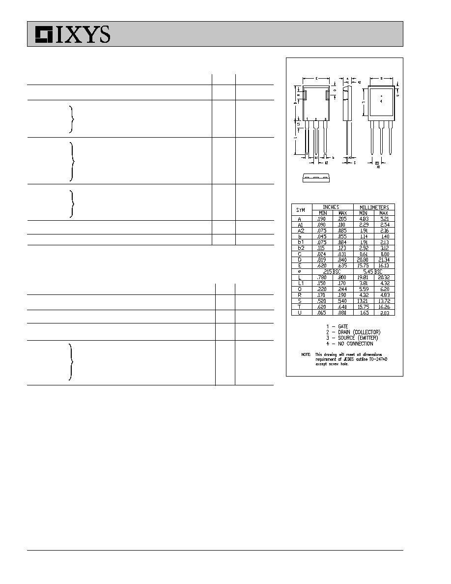
G = Gate
D = Drain
S = Source
* Patent pending
Isolated back surface*
IXFR 58N20Q
V
DSS
= 200 V
I
D25
=
50 A
R
DS(on)
=
40
m
t
rr
200 ns
HiPerFET
TM
Power MOSFETs
ISOPLUS247
TM
Q-Class
(Electrically Isolated Back Surface)
N-Channel Enhancement Mode
Avalanche Rated, High dV/dt
Low Gate Charge and Capacitances
ISOPLUS 247
TM
E153432
Preliminary Data Sheet
IXYS reserves the right to change limits, test conditions, and dimensions.
IXYS MOSFETS and IGBTs are covered by one or more of the following U.S. patents:
4,835,592
4,881,106
5,017,508
5,049,961
5,187,117
5,486,715
6,306,728B1
4,850,072
4,931,844
5,034,796
5,063,307
5,237,481
5,381,025
Symbol
Test Conditions
Characteristic Values
(T
J
= 25
∞
C, unless otherwise specified)
min.
typ.
max.
g
fs
V
DS
= 10 V; I
D
= 29A
Note 2
24
34
S
C
iss
3600
pF
C
oss
V
GS
= 0 V, V
DS
= 25 V, f = 1 MHz
870
pF
C
rss
280
pF
t
d(on)
20
ns
t
r
V
GS
= 10 V, V
DS
= 0.5 V
DSS
, I
D
= 29A
40
ns
t
d(off)
R
G
= 1.5
(External),
40
ns
t
f
13
ns
Q
g(on)
98 140
nC
Q
gs
V
GS
= 10 V, V
DS
= 0.5 V
DSS
, I
D
= 29A
25
35
nC
Q
gd
45
70
nC
R
thJC
0.5
K/W
R
thCK
(TO-247)
0.15
K/W
Source-Drain Diode
Characteristic Values
(T
J
= 25
∞
C, unless otherwise specified)
Symbol
Test Conditions
min.
typ.
max.
I
S
V
GS
= 0 V
58
A
I
SM
Repetitive, Note 1
232
A
V
SD
I
F
= I
s
, V
GS
= 0 V, Note 2
1.5
V
t
rr
200
ns
Q
RM
0.7
µ
C
I
RM
7
A
I
F
= I
s
, -di/dt = 100 A/
µ
s, V
R
= 100 V
Note: 1. Pulse width limited by T
JM
2. Pulse test, t
300
µ
s, duty cycle d
2 %
IXFR 58N20Q
ISOPLUS 247 OUTLINE