1 - 2
© 2000 IXYS All rights reserved
Symbol
Test Conditions
Maximum Ratings
V
DSS
T
J
= 25
∞
C to 150
∞
C
200
V
V
DGR
T
J
= 25
∞
C to 150
∞
C; R
GS
= 1 M
W
200
V
V
GS
Continuous
±
20
V
V
GSM
Transient
±
30
V
I
D25
T
C
= 25
∞
C
71
A
I
DM
T
C
= 25
∞
C, pulse width limited by T
JM
320
A
I
AR
T
C
= 25
∞
C
80
A
E
AR
T
C
= 25
∞
C
45
mJ
E
AS
1.5
J
dv/dt
I
S
£
I
DM
, di/dt
£
100 A/
m
s, V
DD
£
V
DSS
,
5
V/ns
T
J
£
150
∞
C, R
G
= 2
W
P
D
T
C
= 25
∞
C
310
W
T
J
-55 ... +150
∞
C
T
JM
150
∞
C
T
stg
-55 ... +150
∞
C
T
L
1.6 mm (0.063 in) from case for 10 s 300
∞
C
M
d
Mounting torque
1.13/10 Nm/lb.in.
Weight
5
g
N-Channel Enhancement Mode
Avalanche Rated
Low Q
g
,
High dv/dt
Symbol
Test Conditions
Characteristic Values
(T
J
= 25
∞
C, unless otherwise specified)
min.
typ.
max.
V
DSS
V
GS
= 0 V, I
D
= 250 uA
200
V
V
GS(th)
V
DS
= V
GS
, I
D
= 4 mA
2.0
4.0
V
I
GSS
V
GS
=
±
20 V
DC
, V
DS
= 0
±
100
nA
I
DSS
V
DS
= V
DSS
T
J
= 25
∞
C
25
m
A
V
GS
= 0 V
T
J
= 125
∞
C
1
mA
R
DS(on)
V
GS
= 10 V, I
D
= I
T
28
m
W
Note 1
HiPerFET
TM
Power MOSFETs
ISOPLUS247
TM
, Q-Class
(Electrically Isolated Back Surface)
98617A (7/00)
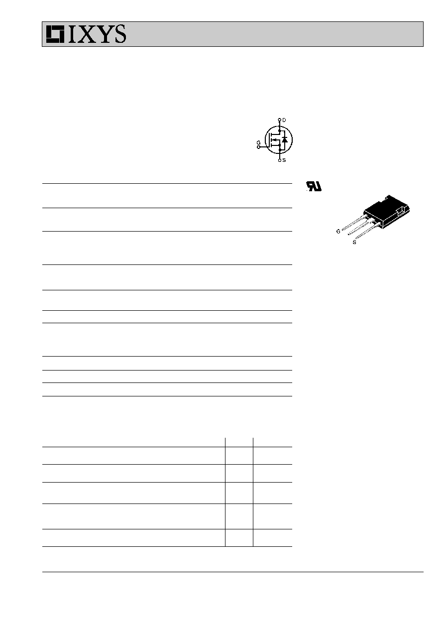
G
D
G = Gate
D = Drain
S = Source
TAB = Drain
Features
∑ Silicon chip on Direct-Copper-Bond
substrate
- High power dissipation
- Isolated mounting surface
- 2500V electrical isolation
∑ Low drain to tab capacitance(<30pF)
∑ Low R
DS (on)
HDMOS
TM
process
∑ Rugged polysilicon gate cell structure
∑ Unclamped Inductive Switching (UIS)
rated
∑ Fast intrinsic Rectifier
Applications
∑ DC-DC converters
∑ Battery chargers
∑ Switched-mode and resonant-mode
power supplies
∑ DC choppers
∑ AC motor control
Advantages
∑ Easy assembly
∑ Space savings
∑ High power density
IXFR 80N20Q
V
DSS
= 200 V
I
D25
= 71 A
R
DS(on)
= 28m
W
t
rr
£
200 ns
ISOPLUS 247
TM
E153432
IXYS reserves the right to change limits, test conditions, and dimensions.
Preliminary data
2 - 2
© 2000 IXYS All rights reserved
Symbol
Test Conditions
Characteristic Values
(T
J
= 25
∞
C, unless otherwise specified)
min.
typ.
max.
g
fs
V
DS
= 10 V; I
D
= I
T
Note 1
35
45
S
C
iss
4600
pF
C
oss
V
GS
= 0 V, V
DS
= 25 V, f = 1 MHz
1100
pF
C
rss
500
pF
t
d(on)
26
ns
t
r
V
GS
= 10 V, V
DS
= 0.5 ∑ V
DSS
, I
D
= I
T
50
ns
t
d(off)
R
G
= 2
W
(External),
75
ns
t
f
20
ns
Q
g(on)
180
nC
Q
gs
V
GS
= 10 V, V
DS
= 0.5 ∑ V
DSS
, I
D
= I
T
39
nC
Q
gd
100
nC
R
thJC
0.40
K/W
R
thCK
0.15
K/W
Source-Drain Diode
Characteristic Values
(T
J
= 25
∞
C, unless otherwise specified)
Symbol
Test Conditions
min.
typ.
max.
I
S
V
GS
= 0 V
80
A
I
SM
Repetitive;
320
A
pulse width limited by T
JM
V
SD
I
F
= I
S
, V
GS
= 0 V, Note 1
1.5
V
t
rr
200
ns
Q
RM
1.2
m
C
I
RM
10
A
I
F
= I
S
, -di/dt = 100 A/
m
s, V
R
= 100 V
Note: 1. Pulse test, t
£
300
m
s, duty cycle d
£
2 %; I
T
= 80A
IXFR 80N20Q
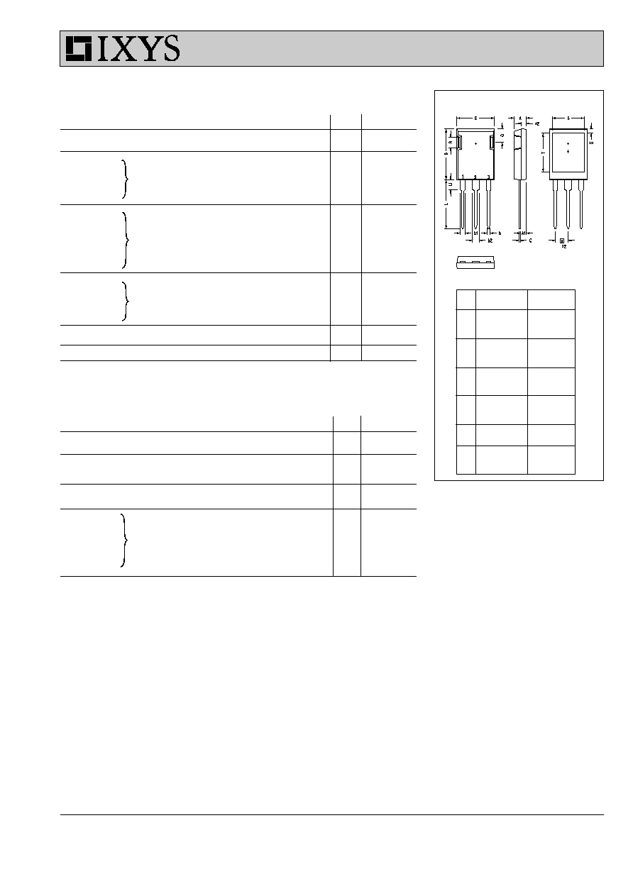
ISOPLUS 247 (IXFR) OUTLINE
Dim.
Millimeter
Inches
Min.
Max.
Min. Max.
A
4.83
5.21
.190 .205
A
1
2.29
2.54
.090 .100
A
2
1.91
2.16
.075 .085
b
1.14
1.40
.045 .055
b
1
1.91
2.13
.075 .084
b
2
2.92
3.12
.115 .123
C
0.61
0.80
.024 .031
D
20.80
21.34
.819 .840
E
15.75
16.13
.620 .635
e 5.45 BSC
.215 BSC
L
19.81
20.32
.780 .800
L1
3.81
4.32
.150 .170
Q
5.59
6.20
.220 .244
R
4.32
4.83
.170 .190
S
13.21
13.72
.520 .540
T
15.75
16.26
.620 .640
U
1.65
3.03
.065 .080
1 Gate, 2 Drain (Collector)
3 Source (Emitter)
4 no connection
IXYS MOSFETS and IGBTs are covered by one or more of the following U.S. patents:
4,835,592
4,881,106
5,017,508
5,049,961
5,187,117
5,486,715
4,850,072
4,931,844
5,034,796
5,063,307
5,237,481
5,381,025