DS99364(IXFH-IXFT-IXFV36N50P)

© 2005 IXYS All rights reserved
Symbol
Test Conditions
Maximum Ratings
V
DSS
T
J
= 25
°C to 175°C
500
V
V
DGR
T
J
= 25
°C to 175°C; R
GS
= 1 M
500
V
V
GS
Continuous
± 30
V
V
GSM
Transient
± 40
V
I
D25
T
C
= 25
°C
36
A
I
DM
T
C
= 25
°C, pulse width limited by T
JM
108
A
I
AR
T
C
= 25
°C
36
A
E
AR
T
C
= 25
°C
50
mJ
E
AS
T
C
= 25
°C
1.5
J
dv/dt
I
S
I
DM
, di/dt
100 A/s, V
DD
V
DSS
,
10
V/ns
T
J
150°C, R
G
= 10
P
D
T
C
= 25
°C
540
W
T
J
-55 ... +150
°C
T
JM
150
°C
T
stg
-55 ... +150
°C
T
L
1.6 mm (0.062 in.) from case for 10 s
300
°C
Maximum tab temperature for soldering
260
°C
for 10s
M
d
Mounting torque(TO-247)
1.13/10 Nm/lb.in.
Weight
TO-247
6
g
TO-268
5 g
PLUS220
2
g
G = Gate
D = Drain
S = Source
TAB = Drain
DS99364D(10/05)
Symbol
Test Conditions
Characteristic Values
(T
J
= 25
°C, unless otherwise specified)
Min. Typ.
Max.
V
DSS
V
GS
= 0 V, I
D
= 4 mA
500
V
V
GS(th)
V
DS
= V
GS
, I
D
= 250
A
3.0
5.0
V
I
GSS
V
GS
=
±20 V
DC
, V
DS
= 0
±100
nA
I
DSS
V
DS
= V
DSS
25
A
V
GS
= 0 V
T
J
= 125
°C
250
A
R
DS(on)
V
GS
= 10 V, I
D
= 0.5 I
D25
170 m
Pulse test, t
300 s, duty cycle d 2 %
PolarHV
TM
HiPerFET
Power MOSFET
Advance Technical Information
N-Channel Enhancement
ModeAvalanche Rated
Fast Intrinsic Diode
Features
International standard packages
Unclamped Inductive Switching (UIS)
rated
Low package inductance
- easy to drive and to protect
Advantages
Easy to mount
Space savings
High power density
IXFH 36N50P
IXFT 36N50P
IXFV 36N50P
IXFV 36N50PS
V
DSS
= 500 V
I
D25
= 36 A
R
DS(on)
= 170 m
TO-247 AD (IXFH)
(TAB)
TO-268 (IXTT)
G
S
D (TAB)
G
S
D
PLUS220 (IXFV)
D (TAB)
G
S
D (TAB)
PLUS220SMD (IXFV...S)
IXYS reserves the right to change limits, test conditions, and dimensions.
IXFH36N50P IXFT 36N50P
IXFV 36N50P
IXYS MOSFETs and IGBTs are covered by 4,835,592
4,931,844
5,049,961
5,237,481
6,162,665
6,404,065 B1
6,683,344
6,727,585
one or moreof the following U.S. patents:
4,850,072
5,017,508
5,063,307
5,381,025
6,259,123 B1
6,534,343
6,710,405B2
6,759,692
4,881,106
5,034,796
5,187,117
5,486,715
6,306,728 B1
6,583,505
6,710,463
6,771,478 B2
Symbol
Test Conditions Characteristic Values
(T
J
= 25
°C, unless otherwise specified)
Min.
Typ.
Max.
g
fs
V
DS
= 20 V; I
D
= 0.5 I
D25
, pulse test
36
S
C
iss
4770
pF
C
oss
V
GS
= 0 V, V
DS
= 25 V, f = 1 MHz
510
pF
C
rss
58
pF
t
d(on)
25
ns
t
r
V
GS
= 10 V, V
DS
= 0.5 V
DSS
, I
D
= I
D25
27
ns
t
d(off)
R
G
= 18
(External)
75
ns
t
f
21
ns
Q
g(on)
134
nC
Q
gs
V
GS
= 10 V, V
DS
= 0.5 V
DSS
, I
D
= 0.5 I
D25
29
nC
Q
gd
64
nC
R
thJC
0.23 K/W
R
thCK
(TO-247)
0.21
K/W
(PLUS220) 0.21 K/W
Source-Drain Diode Characteristic Values
(T
J
= 25
°C, unless otherwise specified)
Symbol
Test Conditions
Min.
typ.
Max.
I
S
V
GS
= 0 V
36
A
I
SM
Repetitive
108
A
V
SD
I
F
= I
S
, V
GS
= 0 V,
1.5
V
Pulse test, t
300 s, duty cycle d 2 %
t
rr
I
F
= 22A,
250
ns
Q
RM
-di/dt = 100 A/
s
0.8
C
I
RM
V
R
= 100V 8.0 A
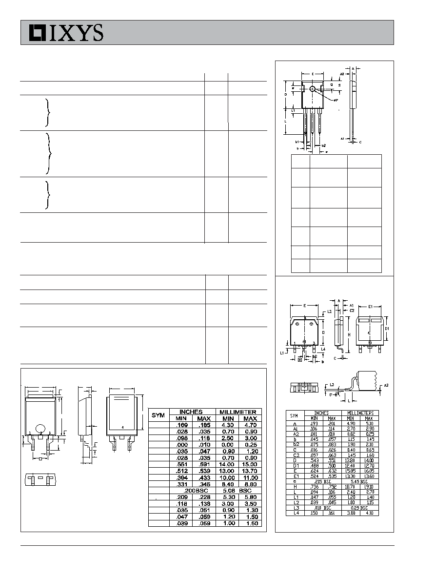
TO-247 AD (IXFH) Outline
Terminals:
1 - Gate
2 - Drain
3 - Source
Tab - Drain
1 2 3
Dim.
Millimeter
Inches
Min.
Max.
Min.
Max.
A
4.7
5.3
.185
.209
A
1
2.2
2.54
.087
.102
A
2
2.2
2.6
.059
.098
b
1.0
1.4
.040
.055
b
1
1.65
2.13
.065
.084
b
2
2.87
3.12
.113
.123
C
.4
.8
.016
.031
D
20.80
21.46
.819
.845
E
15.75
16.26
.610
.640
e
5.20
5.72
0.205
0.225
L
19.81
20.32
.780
.800
L1
4.50
.177
P
3.55
3.65
.140
.144
Q
5.89
6.40
0.232
0.252
R
4.32
5.49
.170
.216
S
6.15
BSC
242
BSC
TO-268 (IXTT) Outline
L
L3
L2
L1
A1
E1
e
D1
E
b
D
c
A2
A
A3
L4
Terminals: 1 - Gate
2 - Drain
3 - Source
TAB - Drain
E
E1
D
L2
A
A1
L1
L
L3
e
2X b
c
A2
L4
A3
E1
PLUS220SMD (IXFV__S) Outline
© 2005 IXYS All rights reserved
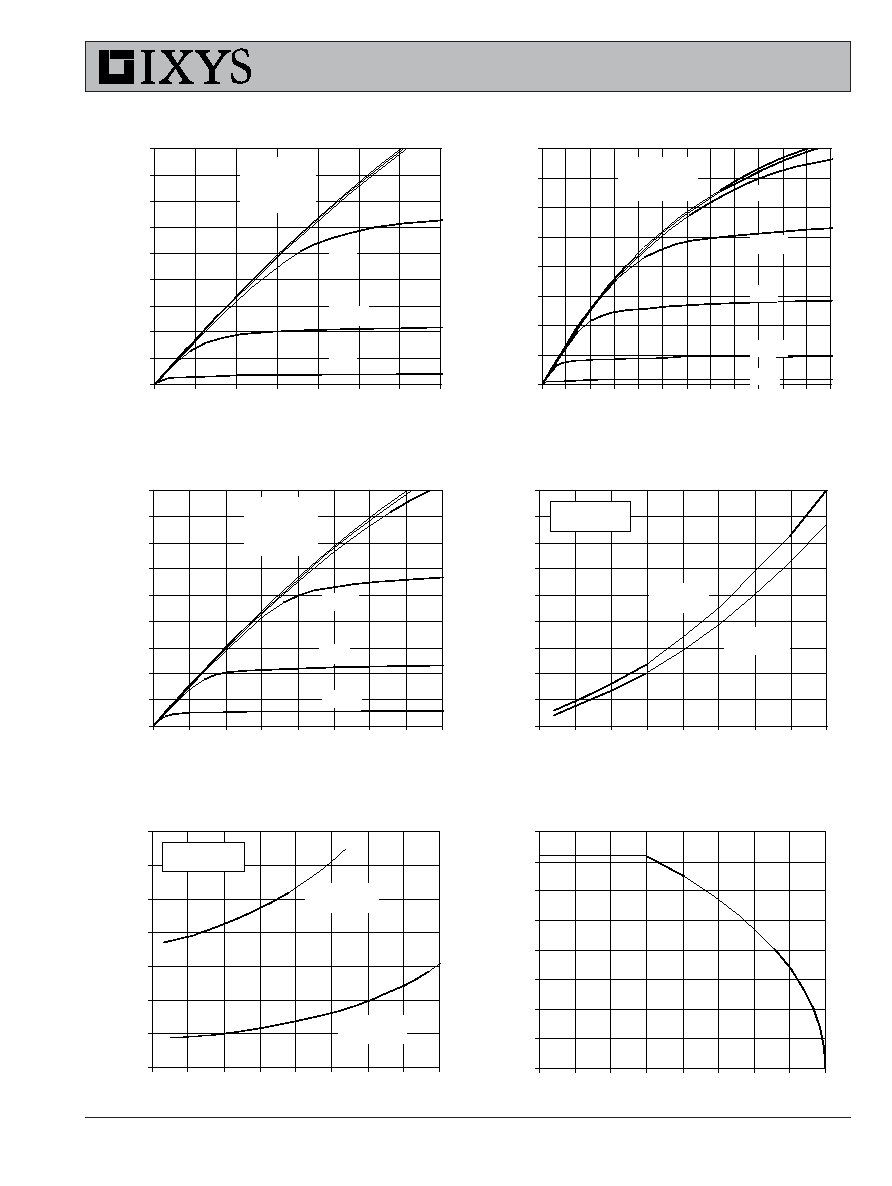
Fig. 2. Extended Output Characteristics
@ 25
º
C
0
10
20
30
40
50
60
70
80
0
2
4
6
8
10
12 14 16 18
20 22 24
V
D S
- Volts
I
D
-
A
m
per
es
V
GS
= 10V
8V
5.5V
5V
6V
6.5V
7V
Fig. 3. Output Characteristics
@ 125
º
C
0
4
8
12
16
20
24
28
32
36
0
2
4
6
8
10
12
14
16
V
D S
- Volts
I
D
-
A
m
per
es
V
GS
= 10V
7V
6V
4.5V
5V
5.5V
Fig. 1. Output Characteristics
@ 25
º
C
0
4
8
12
16
20
24
28
32
36
0
1
2
3
4
5
6
7
V
D S
- Volts
I
D
-
A
m
per
es
V
GS
= 10V
8V
7V
5V
6V
5.5V
Fig. 4. R
DS(on
)
Norm alized to 0.5 I
D25
Value vs. Junction Temperature
0.4
0.7
1
1.3
1.6
1.9
2.2
2.5
2.8
3.1
-50
-25
0
25
50
75
100
125
150
T
J
- Degrees Centigrade
R
D
S
(
o n )
-
N
o
r
m
a
liz
ed
I
D
= 36A
I
D
= 18A
V
GS
= 10V
Fig. 6. Drain Current vs. Case
Temperature
0
5
10
15
20
25
30
35
40
-50
-25
0
25
50
75
100
125
150
T
C
- Degrees Centigrade
I
D
-
A
m
per
e
s
Fig. 5. R
DS(on)
Normalized to
0.5 I
D25
Value vs. I
D
0.6
1
1.4
1.8
2.2
2.6
3
3.4
0
10
20
30
40
50
60
70
80
I
D
- Amperes
R
D
S
(
o n )
-
N
o
r
m
aliz
e
d
T
J
= 125ºC
T
J
= 25ºC
V
GS
= 10V
IXFH36N50P IXFT 36N50P
IXFV 36N50P
IXYS reserves the right to change limits, test conditions, and dimensions.
IXFH36N50P IXFT 36N50P
IXFV 36N50P
IXYS MOSFETs and IGBTs are covered by 4,835,592
4,931,844
5,049,961
5,237,481
6,162,665
6,404,065 B1
6,683,344
6,727,585
one or moreof the following U.S. patents:
4,850,072
5,017,508
5,063,307
5,381,025
6,259,123 B1
6,534,343
6,710,405B2
6,759,692
4,881,106
5,034,796
5,187,117
5,486,715
6,306,728 B1
6,583,505
6,710,463
6,771,478 B2
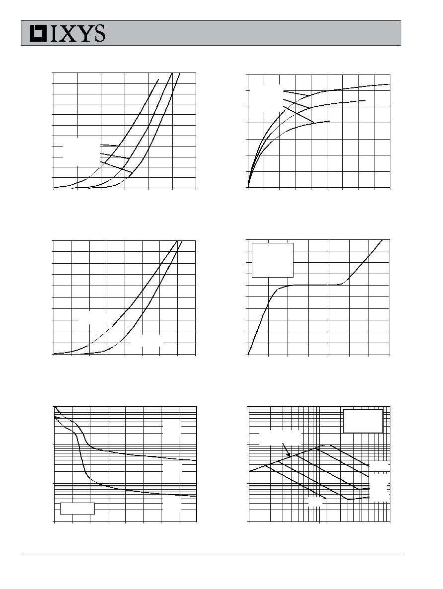
Fig. 11. Capacitance
10
100
1000
10000
0
5
10
15
20
25
30
35
40
V
D S
- Volts
C
a
pa
c
i
t
a
n
c
e
-
pi
c
o
F
a
r
a
ds
Ciss
Coss
Crss
f = 1MHz
Fig. 10. Gate Charge
0
1
2
3
4
5
6
7
8
9
10
0
20
40
60
80
100
120
140
Q
G
- nanoCoulombs
V
G S
- V
o
l
t
s
V
DS
= 250V
I
D
= 18A
I
G
= 10mA
Fig. 7. Input Adm ittance
0
5
10
15
20
25
30
35
40
45
50
55
4
4.5
5
5.5
6
6.5
7
V
G S
- Volts
I
D
- A
m
p
e
re
s
T
J
= 125ºC
25ºC
-40ºC
Fig. 8. Transconductance
0
10
20
30
40
50
60
70
0
10
20
30
40
50
60
70
80
90
I
D
- Amperes
g
f s
-
S
i
e
m
e
n
s
T
J
= -40ºC
25ºC
125ºC
Fig. 9. Source Current vs.
Source-To-Drain Voltage
0
10
20
30
40
50
60
70
80
90
100
0.4
0.5
0.6
0.7
0.8
0.9
1
1.1
1.2
V
S D
- Volts
I
S
-
A
m
p
e
r
e
s
T
J
= 125ºC
T
J
= 25ºC
Fig. 12. Forw ard-Bias
Safe Operating Area
1
10
100
1000
10
100
1000
V
D S
- Volts
I
D
- A
m
p
e
re
s
100s
1ms
DC
T
J
= 150ºC
T
C
= 25ºC
R
DS(on)
Limit
10ms
25s
© 2005 IXYS All rights reserved
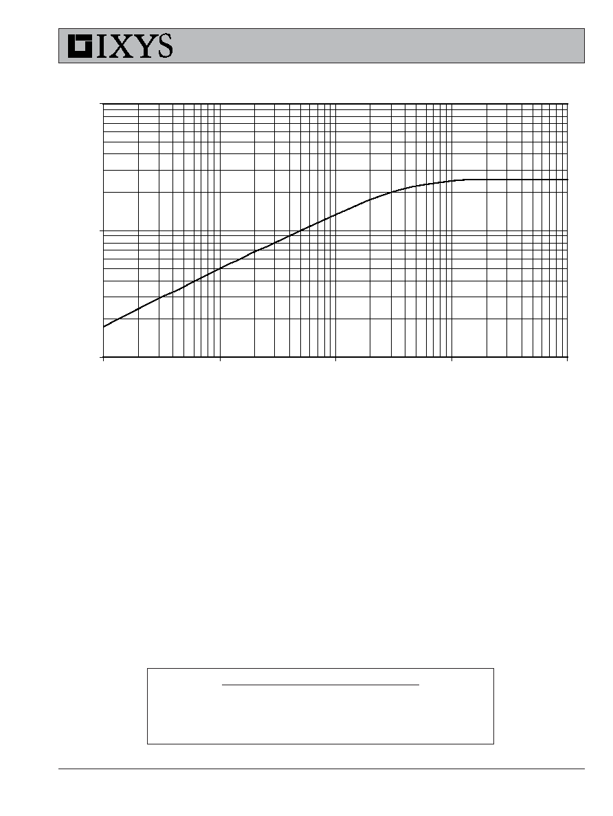
Fig. 13. Maximum Transient Thermal Resistance
0.01
0.10
1.00
0.1
1
10
100
1000
Pulse Width - milliseconds
R
( t h ) J
C
-
º
C / W
IXFH36N50P IXFT 36N50P
IXFV 36N50P
ADVANCE TECHNICAL INFORMATION
The product presented herein is under development. The Technical Specifications offered are
derived from a subjective evaluation of the design, based upon prior knowledge and experience,
and constitute a "considered reflection" of the anticipated objective result. Ixys reserves the right to
change limits, test conditions, and dimensions without notice.