© 2003 IXYS All rights reserved
Symbol
Test Conditions
Maximum Ratings
V
DSS
T
J
= 25
∞C to 150∞C
1000
V
V
DGR
T
J
= 25
∞C to 150∞C; R
GS
= 1 M
1000
V
V
GS
Continuous
±20
V
V
GSM
Transient
±30
V
I
D25
T
C
= 25
∞C
4
A
I
DM
T
C
= 25
∞C, pulse width limited by T
JM
16
A
I
AR
T
C
= 25
∞C
4
A
E
AR
T
C
= 25
∞C
20
mJ
E
AS
700
mJ
dv/dt
I
S
I
DM
, di/dt
100 A/µs, V
DD
V
DSS
, 5 V/ns
T
J
150∞C, R
G
= 2
P
D
T
C
= 25
∞C
150
W
T
J
-55 to +150
∞C
T
JM
150
∞C
T
stg
-55 to +150
∞C
T
L
1.6 mm (0.063 in) from case for 10 s 300
∞C
M
d
Mounting torque
1.13/10 Nm/lb.in.
Weight
TO-247 6
g
TO-268 4
g
N-Channel Enhancement Mode
Avalanche Rated, Low Q
g
,
High dv/dt
Features
IXYS advanced low Q
g
process
Low gate charge and capacitances
- easier to drive
- faster switching
International standard packages
Low R
DS (on)
Unclamped Inductive Switching (UIS)
rated
Molding epoxies meet UL
94
V-0
flammability classification
Advantages
Easy to mount
Space savings
High power density
Symbol
Test Conditions
Characteristic Values
(T
J
= 25
∞C, unless otherwise specified)
min.
typ.
max.
V
DSS
V
GS
= 0 V, I
D
= 1 mA
1000
V
V
GS(th)
V
DS
= V
GS
, I
D
= 1.5 mA
2.5
4.5
V
I
GSS
V
GS
=
±20 V
DC
, V
DS
= 0
±100
nA
I
DSS
V
DS
= V
DSS
T
J
= 25
∞C
50
µA
V
GS
= 0 V
T
J
= 125
∞C
1
mA
R
DS(on)
V
GS
= 10 V, I
D
= 0.5 I
D25
3.0
Pulse test, t
300 µs, duty cycle d 2 %
DS98648C(06/03)
TO-247 AD (IXFH)
G = Gate
D = Drain
S = Source
TAB = Drain
HiPerFET
TM
Power MOSFETs
Q-Class
TO-268 (D3) ( IXFT)
(TAB)
G
S
V
DSS
= 1000 V
I
D25
= 4 A
R
DS(on)
= 3.0
t
rr
250 ns
IXFH 4N100Q
IXFT 4N100Q
(TAB)
G
S
D
IXYS reserves the right to change limits, test conditions, and dimensions.
IXFH 4N100Q
IXFT 4N100Q
IXYS MOSFETs and IGBTs are covered by one or more
of the following U.S. patents:
4,835,592 4,881,106 5,017,508 5,049,961 5,187,117 5,486,715 6,306,728B1 6,259,123B1 6,306,728B1
4,850,072 4,931,844 5,034,796 5,063,307 5,237,481 5,381,025 6,404,065B1 6,162,665 6,534,343
Symbol
Test Conditions
Characteristic Values
(T
J
= 25
∞C, unless otherwise specified)
min.
typ.
max.
g
fs
V
DS
= 20 V; I
D
= 0.5 ∑ I
D25
, pulse test
1.5
2.5
S
C
iss
1050
pF
C
oss
V
GS
= 0 V, V
DS
= 25 V, f = 1 MHz
120
pF
C
rss
30
pF
t
d(on)
17
ns
t
r
V
GS
= 10 V, V
DS
= 0.5 ∑ V
DSS
, I
D
= 0.5 ∑ I
D25
15
ns
t
d(off)
R
G
= 4.7
(External),
32
ns
t
f
18
ns
Q
g(on)
39
nC
Q
gs
V
GS
= 10 V, V
DS
= 0.5 ∑ V
DSS
, I
D
= 0.5 ∑ I
D25
9
nC
Q
gd
22
nC
R
thJC
0.8
K/W
R
thCK
(TO-247)
0.25
K/W
Source-Drain Diode
Characteristic Values
(T
J
= 25
∞C, unless otherwise specified)
Symbol
Test Conditions
min.
typ.
max.
I
S
V
GS
= 0 V
4
A
I
SM
Repetitive; pulse width limited by T
JM
16
A
V
SD
I
F
= I
S
, V
GS
= 0 V,
1.5
V
Pulse test, t
300 µs, duty cycle d 2 %
t
rr
250
ns
Q
RM
I
F
= I
S
, -di/dt = 100 A/
µs, V
R
= 100 V
0.52
µC
I
RM
1.8
A
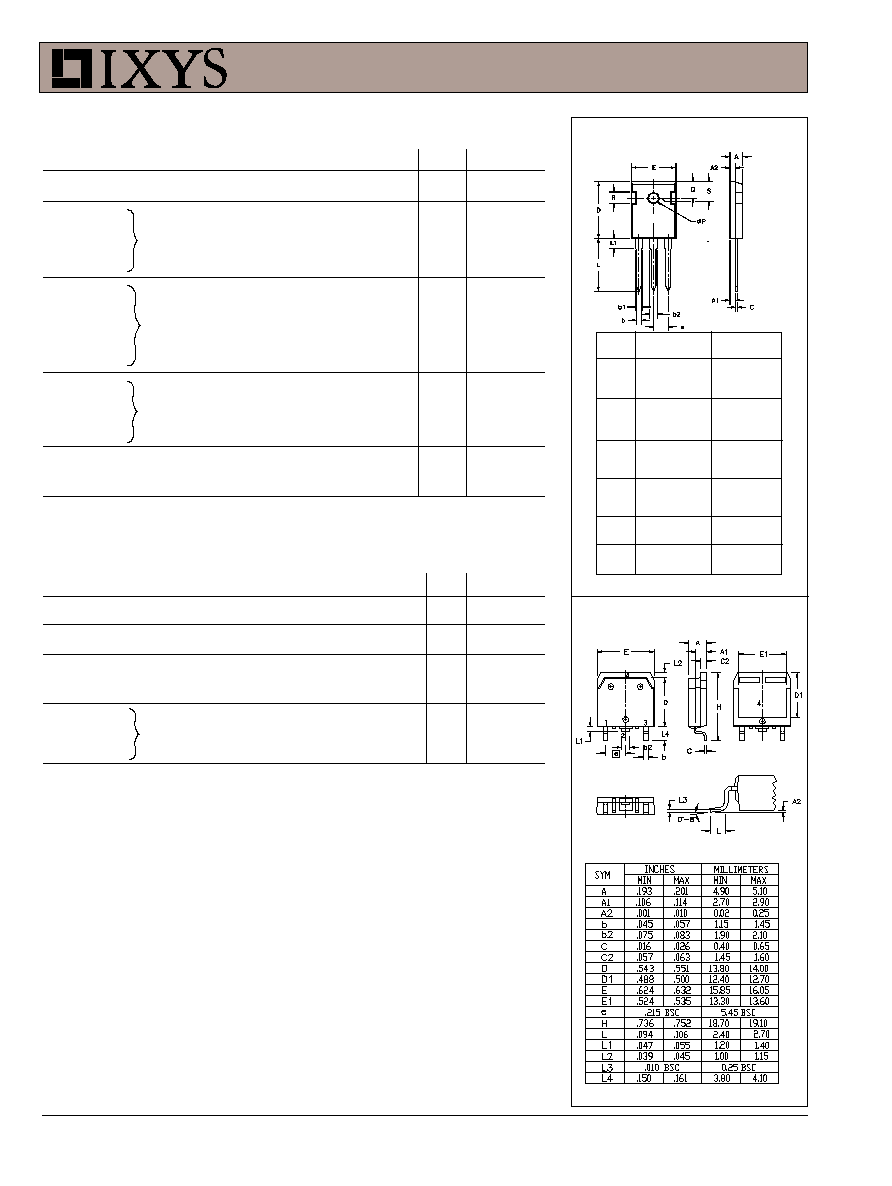
TO-268 Outline
Dim.
Millimeter
Inches
Min.
Max.
Min.
Max.
A
4.7
5.3
.185
.209
A
1
2.2
2.54
.087
.102
A
2
2.2
2.6
.059
.098
b
1.0
1.4
.040
.055
b
1
1.65
2.13
.065
.084
b
2
2.87
3.12
.113
.123
C
.4
.8
.016
.031
D
20.80
21.46
.819
.845
E
15.75
16.26
.610
.640
e
5.20
5.72
0.205
0.225
L
19.81
20.32
.780
.800
L1
4.50
.177
P
3.55
3.65
.140
.144
Q
5.89
6.40
0.232
0.252
R
4.32
5.49
.170
.216
S
6.15 BSC
242 BSC
Terminals:
1 - Gate
2 - Drain
3 - Source
Tab - Drain
1 2 3
TO-247 AD (IXFH) Outline
Terminals: 1 - Gate
2 - Drain
3 - Source
Tab - Drain
© 2003 IXYS All rights reserved
V
DS
- Volts
0
2
4
6
8
10
I
D
-
Am
p
e
re
s
0
1
2
3
4
V
DS
- Volts
0
5
10
15
20
I
D
-
A
m
per
e
s
0
1
2
3
4
T
J
- Degrees C
25
50
75
100
125
150
R
DS
(
O
N
)
- N
o
r
m
aliz
ed
0.8
1.0
1.2
1.4
1.6
1.8
2.0
2.2
2.4
V
GS
- Volts
3
4
5
6
7
8
I
D
-
A
m
per
e
s
0
1
2
3
4
I
D
- Amperes
0
1
2
3
4
5
6
R
DS
(
O
N)
-
N
o
rmaliz
ed
0.8
1.0
1.2
1.4
1.6
1.8
2.0
2.2
2.4
V
CE
- Volts
0
4
8
12
16
20
I
D
-
Am
p
e
re
s
0
1
2
3
4
5
6
7V
6V
VGS = 10V
VGS = 10V
9V
8V
TJ = 25∞C
VGS = 10V
9V
8V
TJ = 25∞C
TJ = 125∞C
5V
5V
TJ = 25∞C
T
J
= 125∞C
6V
7V
5V
6V
7V
VGS = 10V
9V
8V
TJ = 125
O
C
VGS = 10V
ID = 2A
TJ = 25
OC
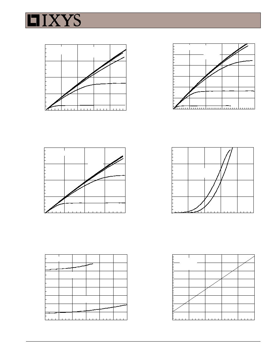
Figure 1. Output Characteristics at 25
O
C
Figure 2. Extended Output Characteristics at 125
O
C
Figure 3. R
DS(on)
normalized to 0.5 I
D25
value vs. I
D
Figure 6. R
DS(on)
normalized to 0.5 I
D25
value vs. T
J
Figure 5. R
DS(on)
normalized to 0.5 I
D25
value vs. I
D
Figure 4. Admittance Curves
IXFH 4N100Q
IXFT 4N100Q
IXYS reserves the right to change limits, test conditions, and dimensions.
IXFH 4N100Q
IXFT 4N100Q
IXYS MOSFETs and IGBTs are covered by one or more
of the following U.S. patents:
4,835,592 4,881,106 5,017,508 5,049,961 5,187,117 5,486,715 6,306,728B1 6,259,123B1 6,306,728B1
4,850,072 4,931,844 5,034,796 5,063,307 5,237,481 5,381,025 6,404,065B1 6,162,665 6,534,343
T
C
- Degrees Centigrade
-50 -25
0
25
50
75 100 125 150
I
D
- A
m
pe
r
e
s
0
1
2
3
4
5
Pulse Width - Seconds
10
-4
10
-3
10
-2
10
-1
10
0
10
1
R(
t
h
)
JC
- K
/
W
0.01
0.10
1.00
V
DS
- Volts
0
5
10
15
20
25
30
35
Ca
pac
i
tanc
e -
pF
10
100
1000
V
SD
- Volts
0.2
0.4
0.6
0.8
1.0
1.2
I
D
- A
m
pe
r
e
s
0
2
4
6
8
10
Gate Charge - nC
0
10
20
30
40
50
60
V
GS
- Vol
t
s
0
3
6
9
12
15
Crss
Coss
Ciss
V
DS
= 600 V
I
D
= 3 A
I
G
= 10 mA
f = 1MHz
T
J
= 125
O
C
T
J
= 25
O
C
60
2000
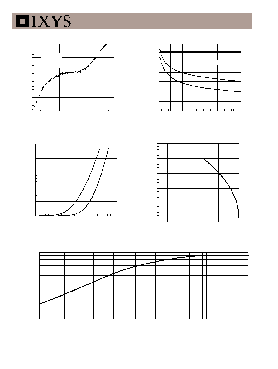
Figure 7. Gate Charge
Figure 8. Capacitance Curves
Figure 9. Forward Voltage Drop of the Intrinsic Diode
Figure10. Drain Current vs. Case Temperature
Figure 11. Transient Thermal Resistance