© 1999 IXYS All rights reserved
Symbol
Test Conditions
Maximum Ratings
V
DSS
T
J
= 25
∞
C to 150
∞
C
1000
V
V
DGR
T
J
= 25
∞
C to 150
∞
C; R
GS
= 1 M
1000
V
V
GS
Continuous
±
20
V
V
GSM
Transient
±
30
V
I
D25
T
C
= 25
∞
C
6
A
I
DM
T
C
= 25
∞
C,
24
A
pulse width limited by T
JM
I
AR
T
C
= 25
∞
C
6
A
E
AR
T
C
= 25
∞
C
20
mJ
E
AS
700
mJ
dv/dt
I
S
I
DM
, di/dt
100 A/
µ
s, V
DD
V
DSS
, 5 V/ns
T
J
150
∞
C, R
G
= 2
P
D
T
C
= 25
∞
C
180
W
T
J
-55 ... +150
∞
C
T
JM
150
∞
C
T
stg
-55 ... +150
∞
C
T
L
1.6 mm (0.063 in) from case for 10 s 300
∞
C
M
d
Mounting torque
1.13/10 Nm/lb.in.
Weight
TO-247 6
g
TO-268 4
g
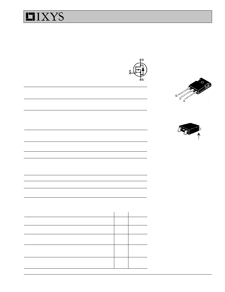
N-Channel Enhancement Mode
Avalanche Rated, Low Q
g
,
High dv/dt
Features
IXYS advanced low Q
g
process
Low gate charge and capacitances
- easier to drive
- faster switching
International standard packages
Low R
DS (on)
Unclamped Inductive Switching (UIS)
rated
Molding epoxies meet UL
94
V-0
flammability classification
Advantages
Easy to mount
Space savings
High power density
Symbol
Test Conditions
Characteristic Values
(T
J
= 25
∞
C, unless otherwise specified)
min.
typ.
max.
V
DSS
V
GS
= 0 V, I
D
= 1 mA
1000
V
V
GS(th)
V
DS
= V
GS
, I
D
= 2.5 mA
2.0
4.5
V
I
GSS
V
GS
=
±
20 V
DC
, V
DS
= 0
±
100
nA
I
DSS
V
DS
= 0.8 V
DSS
T
J
= 25
∞
C
50
µ
A
V
GS
= 0 V
T
J
= 125
∞
C
1
mA
R
DS(on)
V
GS
= 10 V, I
D
= 0.5 I
D25
1.9
Pulse test, t
300
µ
s, duty cycle d
2 %
98561A (6/99)
TO-247 AD (IXFH)
G = Gate
D = Drain
S = Source
TAB = Drain
HiPerFET
TM
Power MOSFETs
Q-Class
TO-268 (D3) ( IXFT)
(TAB)
G
S
V
DSS
= 1000 V
I
D25
= 6 A
R
DS(on)
= 1.9
t
rr
250 ns
IXFH 6N100Q
IXFT 6N100Q
IXYS MOSFETS and IGBTs are covered by one or more of the following U.S. patents:
4,835,592
4,881,106
5,017,508
5,049,961
5,187,117
5,486,715
4,850,072
4,931,844
5,034,796
5,063,307
5,237,481
5,381,025
IXYS reserves the right to change limits, test conditions, and dimensions.
IXFH 6N100Q
IXFT 6N100Q
Symbol
Test Conditions
Characteristic Values
(T
J
= 25
∞
C, unless otherwise specified)
min.
typ.
max.
g
fs
V
DS
= 10 V; I
D
= 0.5 ∑ I
D25
, pulse test
3
5
S
C
iss
2200
pF
C
oss
V
GS
= 0 V, V
DS
= 25 V, f = 1 MHz
180
pF
C
rss
30
pF
t
d(on)
10
ns
t
r
V
GS
= 10 V, V
DS
= 0.5 ∑ V
DSS
, I
D
= 0.5 ∑ I
D25
15
ns
t
d(off)
R
G
= 4.7
(External),
22
ns
t
f
12
ns
Q
g(on)
48
nC
Q
gs
V
GS
= 10 V, V
DS
= 0.5 ∑ V
DSS
, I
D
= 0.5 ∑ I
D25
17
nC
Q
gd
22
nC
R
thJC
0.7
K/W
R
thCK
(TO-247)
0.25
K/W
Source-Drain Diode
Characteristic Values
(T
J
= 25
∞
C, unless otherwise specified)
Symbol
Test Conditions
min.
typ.
max.
I
S
V
GS
= 0 V
9
A
I
SM
Repetitive; pulse width limited by T
JM
24
A
V
SD
I
F
= I
S
, V
GS
= 0 V,
1.5
V
Pulse test, t
300
µ
s, duty cycle d
2 %
t
rr
250
ns
Q
RM
I
F
= I
S
, -di/dt = 100 A/
µ
s, V
R
= 100 V
0.75
µ
C
I
RM
7.5
A
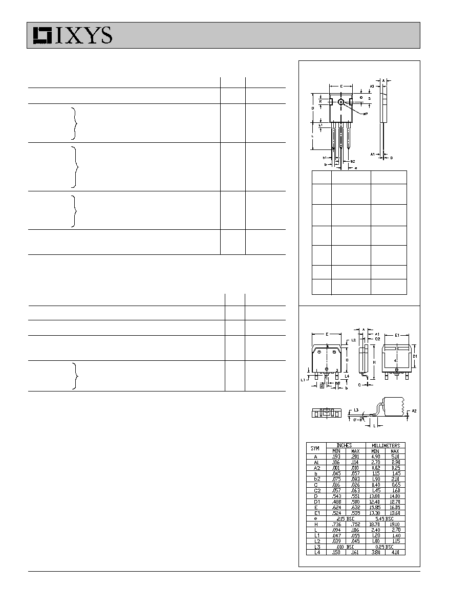
TO-268 Outline
Dim.
Millimeter
Inches
Min.
Max.
Min.
Max.
A
4.7
5.3
.185
.209
A
1
2.2
2.54
.087
.102
A
2
2.2
2.6
.059
.098
b
1.0
1.4
.040
.055
b
1
1.65
2.13
.065
.084
b
2
2.87
3.12
.113
.123
C
.4
.8
.016
.031
D
20.80
21.46
.819
.845
E
15.75
16.26
.610
.640
e
5.20
5.72
0.205
0.225
L
19.81
20.32
.780
.800
L1
4.50
.177
P
3.55
3.65
.140
.144
Q
5.89
6.40
0.232
0.252
R
4.32
5.49
.170
.216
S
6.15 BSC
242 BSC
Terminals:
1 - Gate
2 - Drain
3 - Source
Tab - Drain
1 2 3
TO-247 AD (IXFH) Outline
Terminals: 1 - Gate
2 - Drain
3 - Source
Tab - Drain