© 2000 IXYS All rights reserved
Symbol
Test Conditions
Maximum Ratings
V
DSS
T
J
= 25∞C to 150∞C
200
V
V
DGR
T
J
= 25∞C to 150∞C; R
GS
= 1 MW
200
V
V
GS
Continuous
±20
V
V
GSM
Transient
±30
V
I
D25
T
C
= 25∞C
68N20
68
A
74N20
74
A
I
DM
T
C
= 25∞C, pulse width limited by T
JM
68N20
272
A
74N20
296
A
I
AR
T
C
= 25∞C
68N20
68
A
74N20
74
A
E
AR
T
C
= 25∞C
45
mJ
dv/dt
I
S
£ I
DM
, di/dt £ 100 A/ms, V
DD
£ V
DSS
,
5
V/ns
T
J
£ 150∞C, R
G
= 2 W
P
D
T
C
= 25∞C
360
W
T
J
-55 ... +150
∞C
T
JM
150
∞C
T
stg
-55 ... +150
∞C
T
L
1.6 mm (0.062 in.) from case for 10 s
300
∞C
M
d
Mounting torque
1.13/10 Nm/lb.in.
Weight
6
g
Symbol
Test Conditions
Characteristic Values
(T
J
= 25∞C, unless otherwise specified)
min.typ.max.
V
DSS
V
GS
= 0 V, I
D
= 1 mA
200
V
V
GS(th)
V
DS
= V
GS
, I
D
= 4 mA
2
4
V
I
GSS
V
GS
= ±20 V
DC
, V
DS
= 0
±100
nA
I
DSS
V
DS
= 0.8 V
DSS
T
J
= 25∞C
200
mA
V
GS
= 0 V
T
J
= 125∞C
1
mA
R
DS(on)
V
GS
= 10 V, I
D
= 0.5 I
D25
74N20
30
m W
68N20
35
m W
Pulse test, t £ 300 ms, duty cycle d £ 2 %
HiPerFET
TM
Power MOSFETs
N-Channel Enhancement Mode
High dv/dt, Low t
rr
, HDMOS
TM
Family
TO-247 AD (IXFH)
Features
International standard packages
Low R
DS (on)
HDMOS
TM
process
Rugged polysilicon gate cell structure
Unclamped Inductive Switching (UIS)
rated
Low package inductance
- easy to drive and to protect
Fast intrinsic Rectifier
Applications
DC-DC converters
Synchronous rectification
Battery chargers
Switched-mode and resonant-mode
power supplies
DC choppers
AC motor control
Temperature and lighting controls
Low voltage relays
Advantages
Easy to mount with 1 screw (TO-247)
(isolated mounting screw hole)
High power surface package
High power density
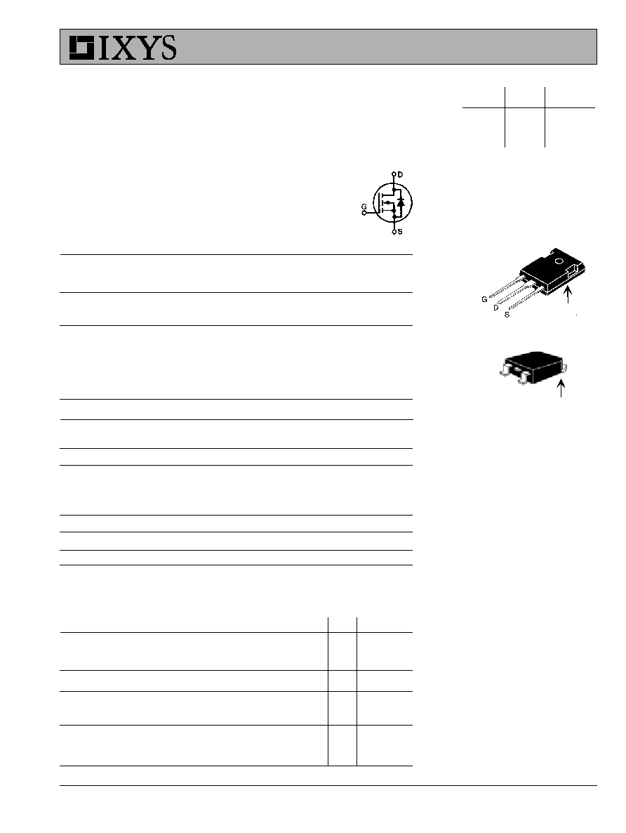
G = Gate,
D = Drain,
S = Source,
TAB = Drain
97522C (8/00)
(TAB)
V
DSS
I
D25
R
DS(on)
IXFH/IXFT 68N20
200 V 68 A 35 mW
IXFH/IXFT 74N20
200 V 74 A 30 mW
t
rr
£ 200 ns
TO-268 (D3) ( IXFT)
(TAB)
G
S
IXYS MOSFETS and IGBTs are covered by one or more of the following U.S. patents:
4,835,592 4,881,106
5,017,508
5,049,961 5,187,117 5,486,715
4,850,072 4,931,844
5,034,796
5,063,307 5,237,481 5,381,025
IXYS reserves the right to change limits, test conditions, and dimensions.
Symbol
Test Conditions
Characteristic Values
(T
J
= 25∞C, unless otherwise specified)
Min. Typ.Max.
g
fs
V
DS
= 10 V; I
D
= 0.5 I
D25
, pulse test
35
45
S
C
iss
5400
pF
C
oss
V
GS
= 0 V, V
DS
= 25 V, f = 1 MHz
1160
pF
C
rss
560
pF
t
d(on)
40
ns
t
r
V
GS
= 10 V, V
DS
= 0.5 V
DSS
, I
D
= 0.5 I
D25
55
ns
t
d(off)
R
G
= 2 W (External)
120
ns
t
f
26
ns
Q
g(on)
280
nC
Q
gs
V
GS
= 10 V, V
DS
= 0.5 V
DSS
, I
D
= 0.5 I
D25
39
nC
Q
gd
135
nC
R
thJC
0.35
K/W
R
thCK
(TO-247 Package)
0.25
K/W
IXFH68N20 & IXFH74N80 characteristic curves can be found in the IXFK72N20/
IXFK80N20 data sheet.
Source-Drain Diode
Characteristic Values
(T
J
= 25∞C, unless otherwise specified)
Symbol
Test Conditions
Min.
Typ. Max.
I
S
V
GS
= 0 V
68N20
68
A
74N20
74
A
I
SM
Repetitive;
68N20
272
A
pulse width limited by T
JM
74N20
296
A
V
SD
I
F
= I
S
, V
GS
= 0 V,
1.5
V
Pulse test, t £ 300 ms, duty cycle d £ 2 %
t
rr
200
ns
Q
RM
0.85
mC
8
A
I
RM
I
F
= 25A
-di/dt = 100 A/ms,
V
R
= 100 V
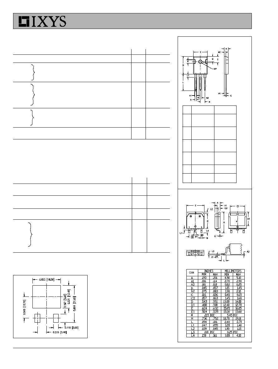
TO-247 AD (IXFH) Outline
Dim.
Millimeter
Inches
Min.
Max.
Min. Max.
A
4.7
5.3
.185
.209
A
1
2.2
2.54
.087
.102
A
2
2.2
2.6
.059
.098
b
1.0
1.4
.040
.055
b
1
1.65
2.13
.065
.084
b
2
2.87
3.12
.113
.123
C
.4
.8
.016
.031
D
20.80 21.46
.819
.845
E
15.75 16.26
.610
.640
e
5.20
5.72 0.205 0.225
L
19.81 20.32
.780
.800
L1
4.50
.177
∆P
3.55
3.65
.140
.144
Q
5.89
6.40 0.232 0.252
R
4.32
5.49
.170
.216
S
6.15 BSC
242 BSC
Terminals:
1 - Gate
2 - Drain
3 - Source
Tab - Drain
1 2 3
TO-268 Outline
IXFH 68N20 IXFH 74N20
IXFT 68N20 IXFT 74N20
Min Recommended Footprint